
Chip to chip interface for interconnecting chips

a chip and interconnecting chip technology, applied in the field of communication networks, can solve the problems of degrading the performance and reliability of the asic, chips often present additional challenges with respect, and the number of i/os can only be implemented in the finite number of i/os, etc., to achieve the effect of reducing the number of i/o pins

Inactive Publication Date: 2005-06-21
GLOBALFOUNDRIES INC
View PDF11 Cites 69 Cited by
  • Summary
  • Abstract
  • Description
  • Claims
  • Application Information

AI Technical Summary

Benefits of technology

[0015]When the Macros are on different chips the signals are transmitted over I / O interfaces. The present invention minimizes the number of I / O pins required to transmit the information between pairs of macros located on different chips. The Chip to Chip Macro of the present invention intercepts request signals generated by other macros, on one chip wishing to communicate with paired macros on another chip. The Chip to Chip Macro forms a data packet that is transmitted via the Chip to Chip Interface Bus to the Chip to Chip Macro on the other chip which converts the data packet to electrical signals and forwards the signals to the paired Chip to Chip Macro.

Problems solved by technology

Unfortunately ASIC packaging technology can implement only a finite number of I / Os.
As the number of I / Os on an ASIC package is increased beyond a practical limit, it creates electrical and mechanical problems that degrade the performance and reliability of the ASIC.
But splitting one ASIC chip into multiple ASICs chips often presents additional challenges with respect to the number of I / Os then required for communication between each of the ASICs in addition to the I / Os required by the originally intended external interfaces.

Method used


Image

  • Chip to chip interface for interconnecting chips
  • Chip to chip interface for interconnecting chips
  • Chip to chip interface for interconnecting chips

Examples


Embodiment Construction

[0027]The above cross reference patent application is fully incorporated herein by reference and, if required, forms part of the disclosure for the present invention.

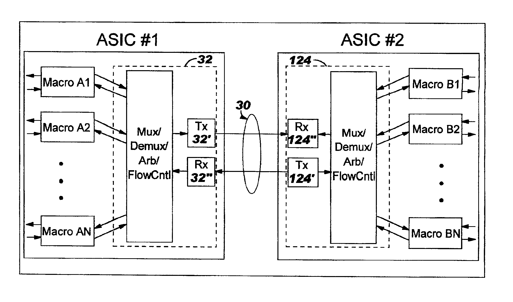
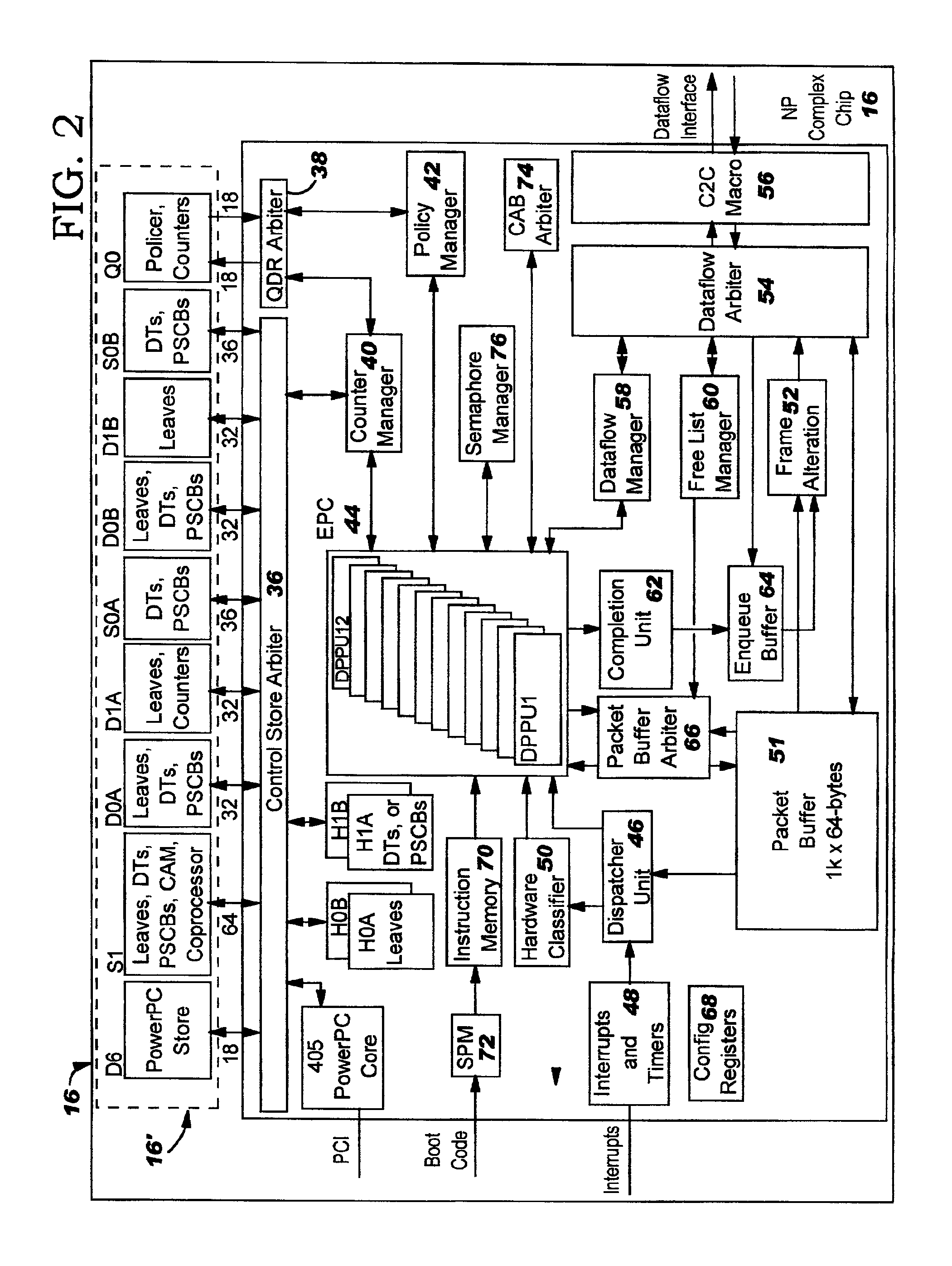
[0028]The present invention provides a Chip to Chip (C2C) Macro 56 (FIG. 2) which is mounted on the Network Processor chip, the Data Flow Chip or the Scheduler Chip and provide a facility for communications between the chips. The chips are interconnected to form a Network Processor. The portions of the referenced application describing the Network Processor and the respective chips forming said Network Processor are reproduced followed by a description of the Chip to Chip Macro and Chip to Chip Interface Bus.

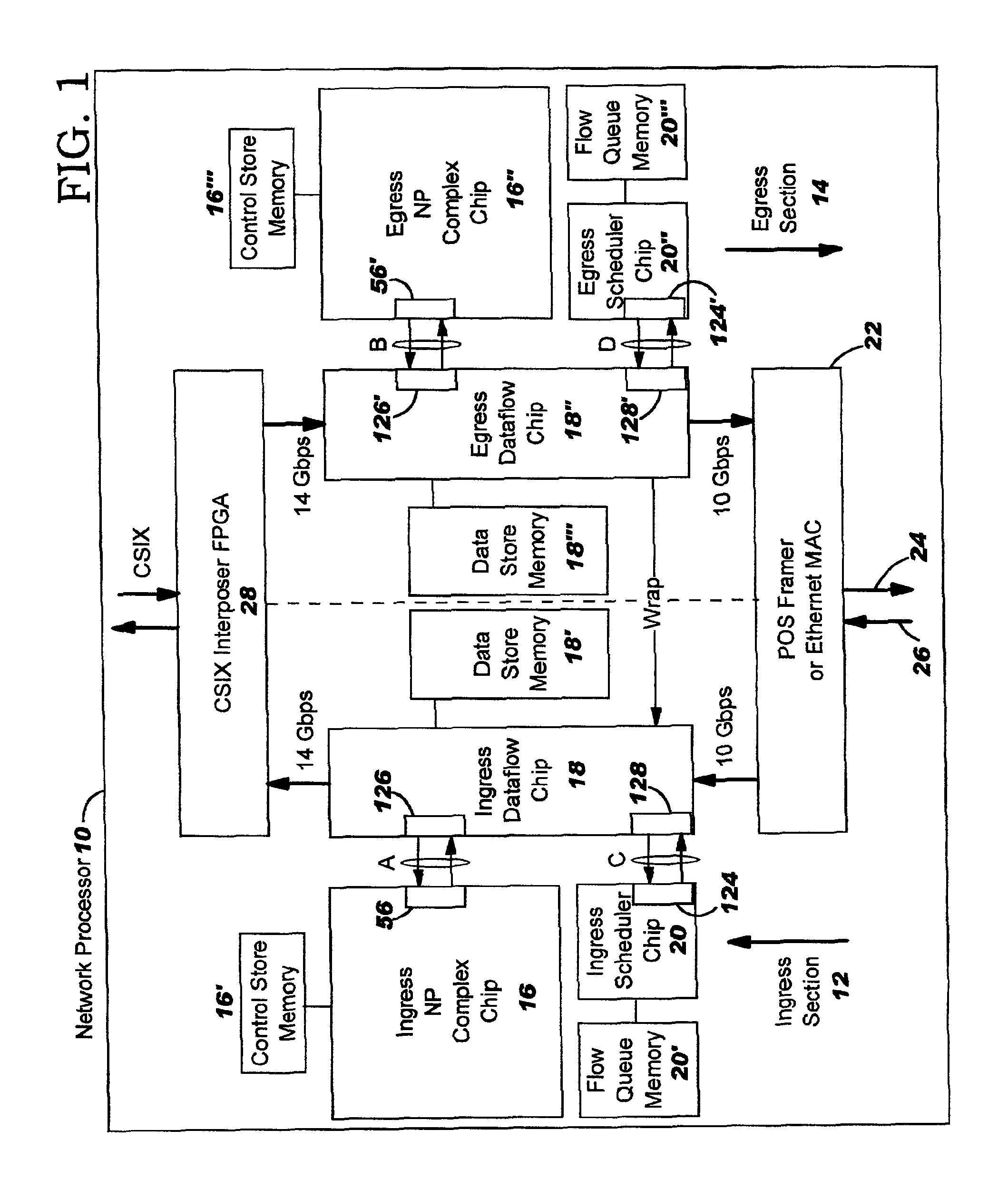
[0029]FIG. 1 shows a block diagram of a Network Processor according to the teachings of the present invention. The Network Processor 10 includes an Ingress section 12 and Egress section 14 symmetrically arranged into a symmetrical structure. The Ingress section includes Ingress Network Processor (NP) Complex Chip 16...


PUM


Abstract

A Network Processor (NP) is formed from a plurality of operatively coupled chips. The NP includes a Network Processor Complex (NPC) Chip coupled to a Data Flow Chip and Data Store Memory coupled to the Data Flow Chip. An optional Scheduler Chip is coupled to the Data Flow Chip. The named components are replicated to create a symmetric ingress and egress structure. Communications between the chips are provided by a pair of Chip to Chip Macros, one of each operatively positioned on one of the chips, and a Chip to Chip Bus Interface operatively coupling the Chip to Chip Macros.

Description

CROSS-REFERENCE TO RELATED PATENT APPLICATIONS[0001]The present application relates to patent application Ser. No. 09 / 838,395, “High Speed Network Processor” which is assigned to the assignee of the present invention. The patent application Ser. No. 09 / 838,395 “High speed Network Processor” describes a high performance network processor formed from multiple interconnected chips and is fully incorporated herein by reference.[0002]The present application describes and claims an interface macro which can be used to interconnect the chips of the “High Speed Network Processor”.BACKGROUND OF THE INVENTION[0003]a) Field of the Invention[0004]The present invention relates to communications networks in general and in particular to circuits used to interconnect chips or modules of a communication system.[0005]b) Prior Art[0006]The ever-increasing requirement for higher performance and data throughput in networking and computing applications creates the need for Application Specific Integrated...

Claims


Application Information

Patent Timeline
Patent Type & Authority Patents(United States)
IPC IPC(8): G06F13/00G06F13/14G06F13/42
CPCG06F13/4265
Inventor CALVIGNAC, JEAN LOUISHEDDES, MARCOIMMING, KERRY CHRISTOPHERLOGAN, JOSEPH FRANKLINOZGUNER, TOLGA
Owner GLOBALFOUNDRIES INC
Features
  • Generate Ideas
  • Intellectual Property
  • Life Sciences
  • Materials
  • Tech Scout
  • Unparalleled Data Quality
  • Higher Quality Content
  • 60% Fewer Hallucinations
Learn More