Method for cutting semiconductor wafer protecting sheet

a technology of protecting sheet and semiconductor, which is applied in the direction of grinding machine components, manufacturing tools, and abrasive surface conditioning devices, etc. it can solve the problems of deterioration of machining performance, damage to wafer b>1/b>, and bad effect of wafer, so as to reduce machining efficiency and quality, and thin finishing thickness

Inactive Publication Date: 2005-06-28
TOKYO SEIMITSU
View PDF17 Cites 14 Cited by
  • Summary
  • Abstract
  • Description
  • Claims
  • Application Information

AI Technical Summary

Benefits of technology

[0014]According to the present invention, the protecting sheet is cut in a required minimum size for protecting the obverse of the wafer, so that the protecting sheet is not included inside a removed portion in a grinding process of the reverse of the wafer even if the wafer is ground to have extremely thin finishing thickness. Hence, the protecting sheet is no

Problems solved by technology

Then, the micro cracks generated at the edge can develop toward the inside of the wafer 1 and the micro fragments can have a bad effect on the wafer 1, and the wafer 1 can

Method used


Image

  • Method for cutting semiconductor wafer protecting sheet
  • Method for cutting semiconductor wafer protecting sheet
  • Method for cutting semiconductor wafer protecting sheet

Examples


Embodiment Construction

[0022]Hereunder a preferred embodiment will be described of the method for cutting the wafer protecting sheet of the present invention with reference to the accompanying drawings.

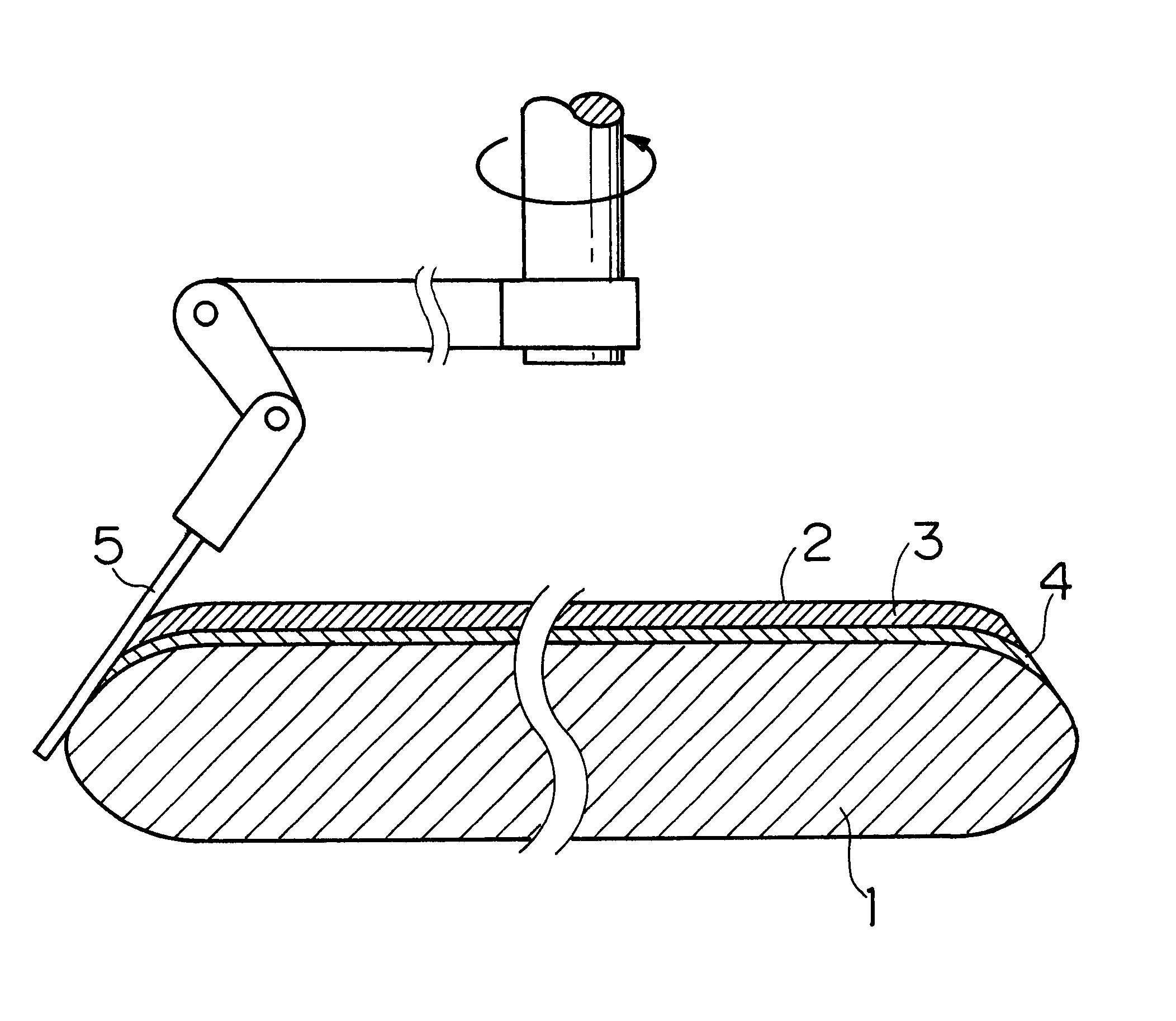
[0023]FIG. 1 is a sectional side view schematically showing a semiconductor wafer 1, on which a protecting sheet 2 is adhered and cut in a cutting method according to an embodiment of the present invention. In FIG. 1, the wafer 1 is mounted and fixed with suction with the reverse down and the obverse, on which semiconductor devices have been formed, up on a stage of a protecting sheet adhering apparatus (not shown).

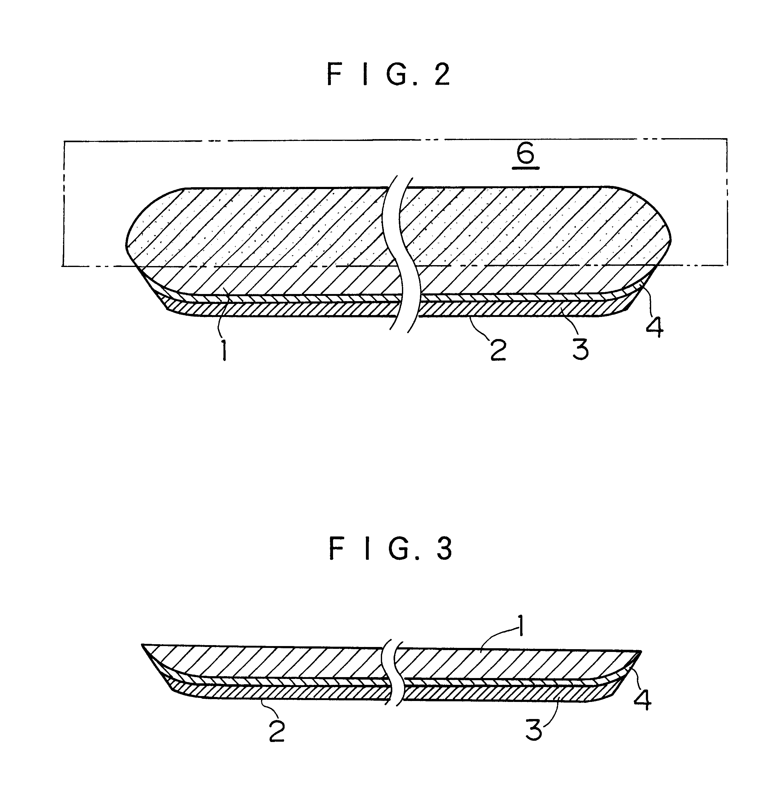
[0024]The protecting sheet 2 is composed of a plastic base 3 and an adhesive layer 4. The protecting sheet 2 is arranged over the wafer 1 with a side of the adhesive layer 4 down, and the protecting sheet 2 is pressed by an elastic body such as a roller and is thereby adhered on the obverse of the wafer 1. At this point, the protecting sheet 2 is adhered in such a manner that the protecting sheet...


PUM

PropertyMeasurementUnit
Thicknessaaaaaaaaaa

Abstract

To cut a protecting sheet adhered over the obverse of a wafer, an inclination angle of a cutting tool is adjusted according to a form of a chamfered part of the wafer and a finishing thickness of the wafer so that the protecting sheet is cut into the required minimum size for protecting the obverse of the wafer. Thus, the protecting sheet is not included inside a removed portion in a grinding process of the reverse of the wafer with a grindstone even if the wafer is ground to have extremely thin finishing thickness. Hence, the protecting sheet is not ground while the reverse of the wafer is ground, and the grindstone is thus prevented from being clogged up with ground material of the protecting sheet.

Description

BACKGROUND OF THE INVENTION[0001]1. Field of the Invention[0002]The present invention relates generally to a method for cutting a wafer protecting sheet, particularly to a method for cutting an obverse protecting sheet that is used for a semiconductor wafer when machining with a back grinder and the like.[0003]2. Description of Related Art[0004]FIG. 4 is a sectional side view of a semiconductor wafer 1, on which a protecting sheet 2 is adhered and cut in a conventional cutting method. Semiconductor devices such as ICs are formed on the obverse of the wafer 1 and are individually inspected, and the wafer 1 is then diced with a dicing saw to separate devices. The semiconductor devices for IC cards and the like are required to be thin. In order to produce the devices of a desired thickness, the reverse of the wafer 1 is ground as shown in FIG. 5 with a back grinder (not shown) before the wafer 1 is diced into the separate devices with the dicing saw. FIG. 6 is a sectional side view of ...

Claims


Application Information

Patent Timeline
IPC IPC(8): H01L21/68H01L21/70H01L21/67H01L21/78H01L21/301H01L21/304
CPCH01L21/6836H01L21/78H01L2221/68327Y10T83/05
Inventor ISHIKAWA, TOSHIHIKOKATAGIRI, YASUSHI
Owner TOKYO SEIMITSU
Why Eureka
Try Eureka