Reducing reset noise in CMOS image sensors

a technology of cmos image sensor and reset noise, which is applied in the field of solid-state imaging devices, can solve the problems of reducing the total charge that can be collected, noise present in the images produced by such devices, and noise associated with conventional cmos image sensor noise, and achieve the effect of reducing reset nois

Active Publication Date: 2005-06-28
RE SECURED NETWORKS LLC
View PDF1 Cites 58 Cited by
  • Summary
  • Abstract
  • Description
  • Claims
  • Application Information

AI Technical Summary

Benefits of technology

[0009]According to one embodiment, during a hard reset operation involving the photodiode, the reset drain voltage circuitry supplies a first drain voltage to the drain of the reset transistor in accordance with a determined level of light for exposure, which is determined dynamically, and the reset gate voltage circuitry supplies a first gate voltage to the gate of the reset transistor such that the first gate voltage is greater than a sum of the first drain voltage and a threshold voltage of the reset transistor. This particular reset operation improves low light photography by reducing reset noise without sacrificing dynamic range.
[0010]According to another embodiment of the present invention, a reset operation involves a first “hard reset” phase followed by a second “soft reset” phase. During the first phase, the reset drain voltage circuitry supplies a first drain voltage to the drain of the reset transistor, and the reset gate voltage circuitry supplies a first gate voltage to the gate of the reset transistor such that the first gate voltage is greater than a sum of the first drain voltage and a threshold voltage of the reset transistor. During the second phase of the reset operation, the reset drain voltage circuitry supplies a second drain voltage to the drain, and reset gate voltage circuitry supplies a second gate voltage to the gate so that the reset transistor performs sub-threshold conduction. This reset process results in significantly reduced reset noise and significantly eliminates image lag without sacrificing or reducing dynamic range.

Problems solved by technology

A significant problem associated with conventional CMOS image sensors is the noise present in the images produced by such devices.
For example, conventional CMOS image sensors suffer from noise associated with the process for resetting the photodiode in each pixel to a known potential after each exposure and in preparation for the next image.
Reducing the capacitance of the sense node can reduce reset noise, but results in a corresponding reduction in the total charge that can be collected and therefore undesirably reduces the overall dynamic range in the camera system.

Method used


Image

  • Reducing reset noise in CMOS image sensors
  • Reducing reset noise in CMOS image sensors
  • Reducing reset noise in CMOS image sensors

Examples


Embodiment Construction

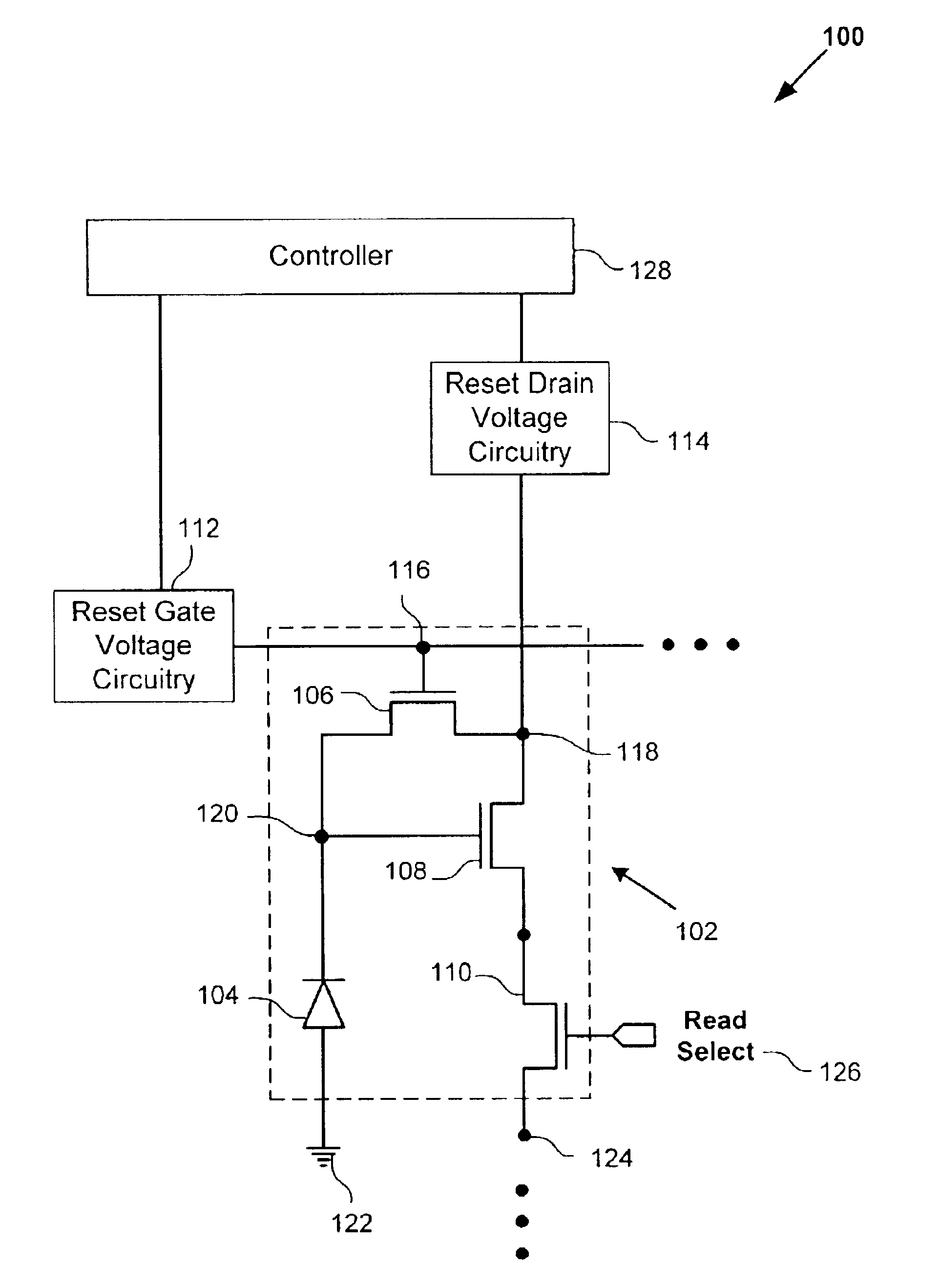
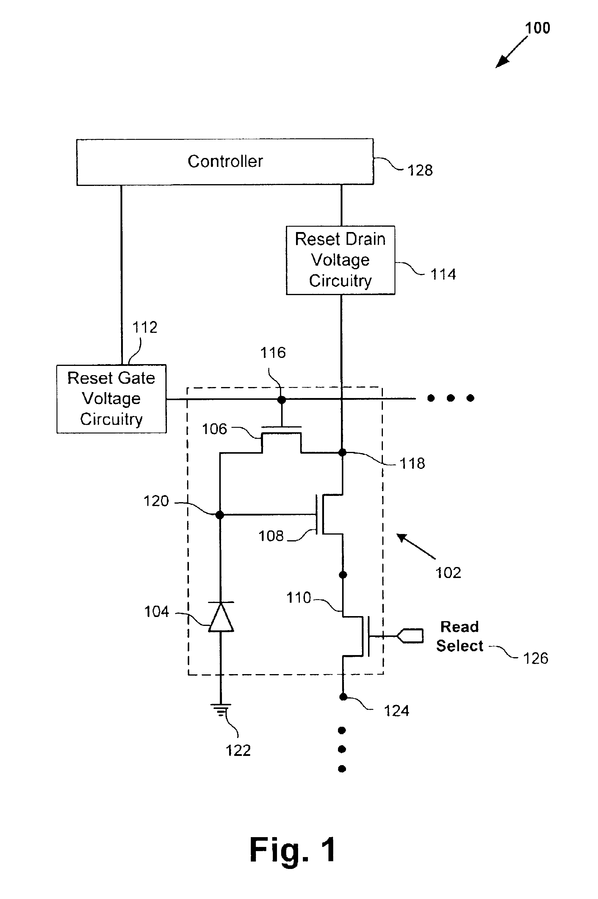
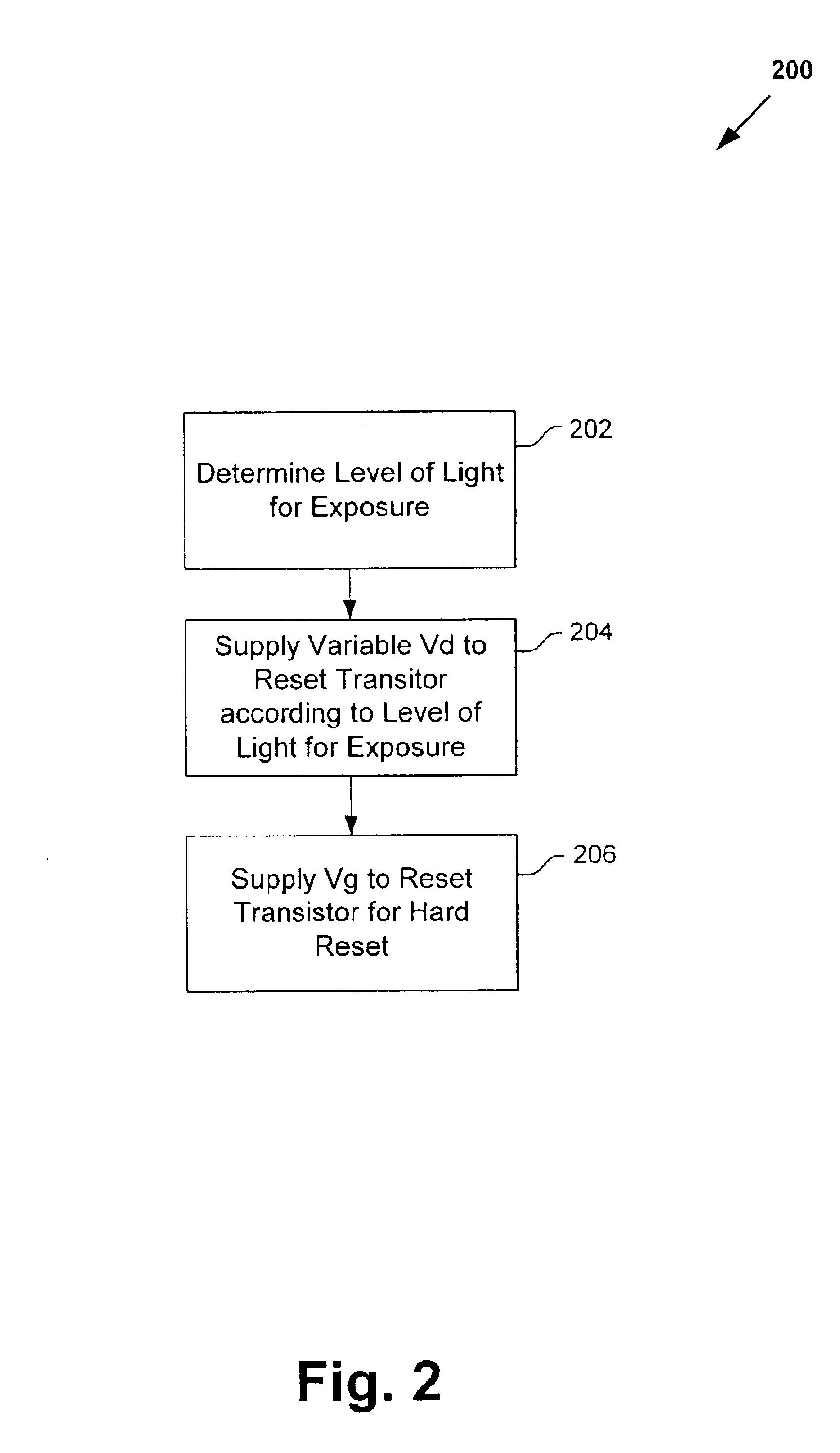
[0019]The present invention is directed to a method of reducing reset noise in a CMOS image sensor. The following description contains specific information pertaining to the implementation of the present invention. One skilled in the art will recognize that the present invention may be implemented in a manner different from that specifically discussed in the present application. Moreover, some of the specific details of the invention are not discussed in order to not obscure the invention. The specific details not described in the present application are within the knowledge of a person of ordinary skill in the art.

[0020]The drawings in the present application and their accompanying detailed description are directed to merely exemplary embodiments of the invention. To maintain brevity, other embodiments of the invention which use the principles of the present invention are not specifically described in the present application and are not specifically illustrated by the present drawi...


PUM


Abstract

An exemplary CMOS image sensor comprises a reset transistor, a photodiode, reset drain voltage circuitry, and reset gate voltage circuitry. A cathode of the photodiode is connected to a source of the reset transistor, and an anode of the photodiode is connected to ground. The reset drain voltage circuitry is connected to a drain of the reset transistor, and the reset gate voltage circuitry is connected to a gate of the reset transistor. During an exemplary hard reset operation, the reset drain voltage circuitry supplies a first drain voltage to the drain of the reset transistor in accordance with a determined level of light for exposure, which is determined dynamically. According to another exemplary reset operation, a hard reset phase is immediately followed by a soft reset phase.

Description

RELATED APPLICATIONS[0001]The present application claims the benefit of U.S. provisional patent application Ser. No. 60 / 376,748, filed Apr. 30, 2002, which is hereby fully incorporated by reference in the present application.BACKGROUND OF THE INVENTION[0002]1. Field of the Invention[0003]The present invention is generally in the field of solid state imaging devices. More specifically, the invention is in the field of Complementary Metal Oxide Semiconductor (“CMOS”) imaging devices.[0004]2. Related Art[0005]CMOS image sensors are increasingly used in a variety of electronic systems and applications to provide motion picture or still picture capability. CMOS image sensors offer a number of technical advantages over alternative devices, such as low power consumption, high level of integration (and corresponding low total system cost), and flexible operating modes, among others.[0006]A significant problem associated with conventional CMOS image sensors is the noise present in the images...

Claims


Application Information

Patent Timeline
Patent Type & Authority Patents(United States)
IPC IPC(8): H04N3/14H04N5/363H04N5/374
CPCH04N5/363H04N5/3597H04N25/626H04N25/65
Inventor BENCUYA, SELIMMANN, RICHARDTAY, HIOK-NAM
Owner RE SECURED NETWORKS LLC
Why Eureka
Try Eureka