Photoelectric conversion device and electronic device having the same

a technology of electronic devices and conversion devices, applied in the field of photoelectric conversion devices, can solve the problems of inability to obtain a wide dynamic range, and achieve the effects of wide application illuminance range, low illuminance, and high illuminan

Active Publication Date: 2009-01-29
SEMICON ENERGY LAB CO LTD
View PDF45 Cites 42 Cited by
  • Summary
  • Abstract
  • Description
  • Claims
  • Application Information

AI Technical Summary

Benefits of technology

[0007]In order to solve the above-described problem, a photoelectric conversion device of the present invention enables an applicable illuminance range to be widened by providing a plurality of transistors in parallel whose ratios of channel length L to channel width W, α=W / L, are different from each other as transistors on the output side (hereinafter referred to as output side transistors) of a current mirror circuit which amplifies a photocurrent.
[0008]In the photoelectric conversion device of the present invention, a plurality of transistors whose ratios of channel length L to channel width W, α=W / L, are different from each other are provided in parallel as output side transistors of a current mirror circuit which amplifies a photocurrent. When an internal resistor is connected to each of the output side transistors in series and the total sum of currents which flow through the plurality of transistors is output, a transistor with large amount of a can be driven with low illuminance in a linear region, and a transistor with small amount of a can be driven with high illuminance in a linear region; by using this, the photoelectric conversion device of the present invention can have a wider applicable illuminance range.

Problems solved by technology

Therefore, there is a problem in that wide dynamic range cannot be obtained.

Method used


Image

  • Photoelectric conversion device and electronic device having the same
  • Photoelectric conversion device and electronic device having the same
  • Photoelectric conversion device and electronic device having the same

Examples


embodiment mode 1

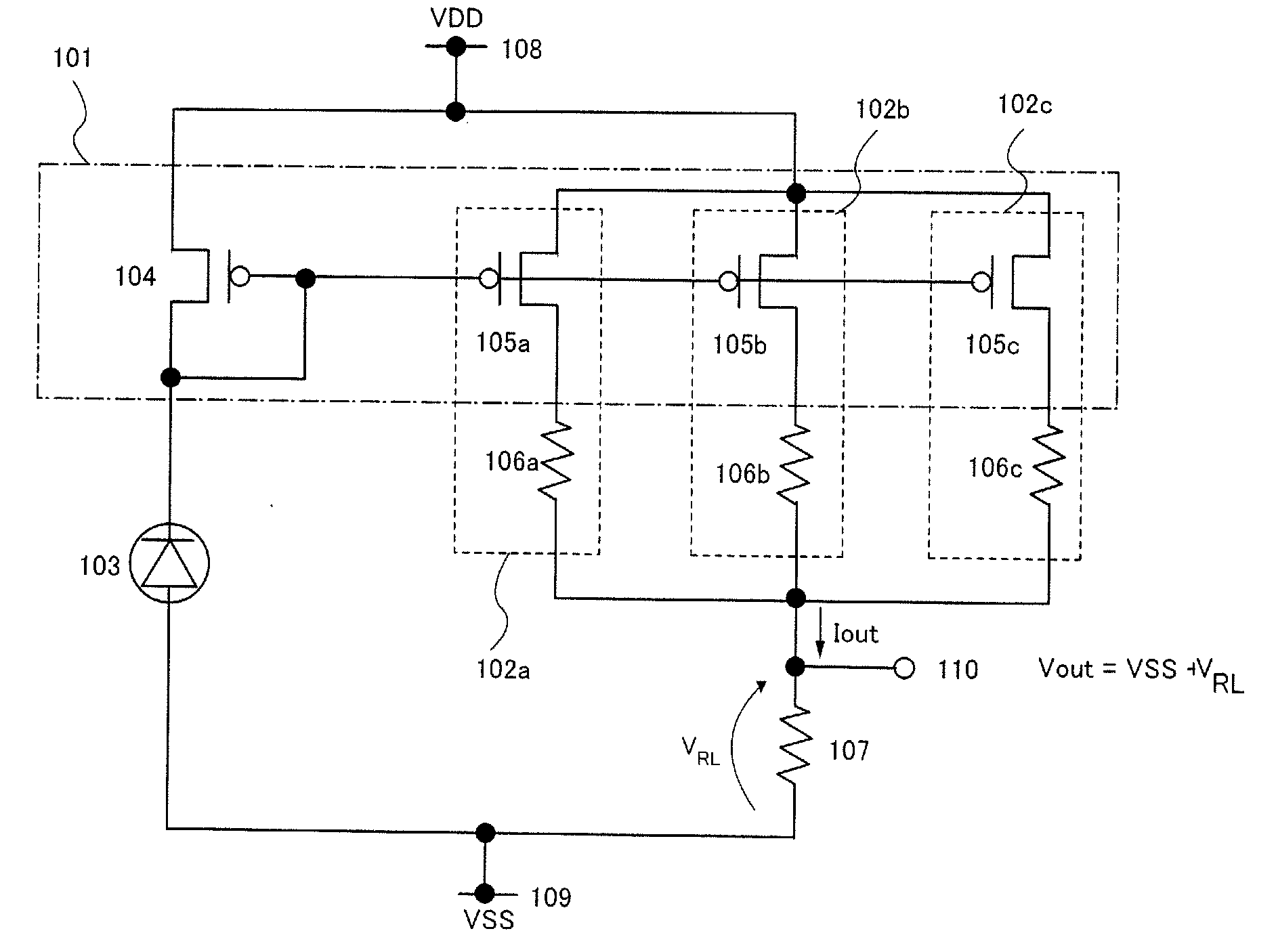
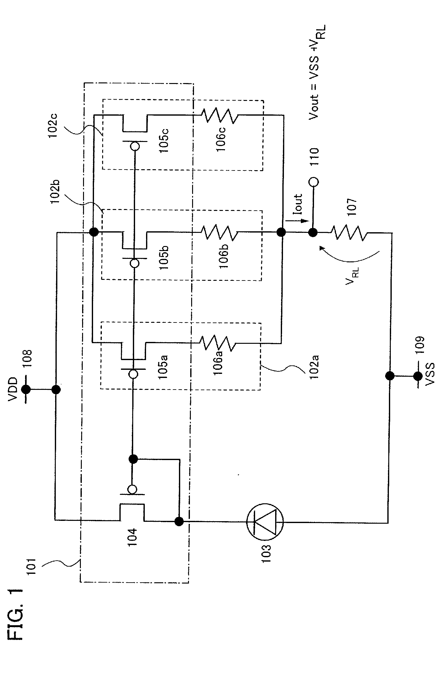
[0035]This embodiment mode will be described with reference to accompanying drawings. FIG. 1 illustrates a circuit configuration of a photoelectric conversion device in Embodiment Mode 1 of the present invention.

[0036]The photoelectric conversion device in this embodiment mode includes a photoelectric conversion element 103, a current mirror circuit 101 which is an amplifier circuit for amplifying an output current (also referred to as a photocurrent) from the photoelectric conversion element 103, three internal resistors 106a to 106c, a load resistor 107, a high potential side power supply line 108, a low potential side power supply line 109, and an output terminal 110. The current mirror circuit 101 includes a reference side transistor 104 and three output side transistors 105a to 105c.

[0037]Note that in FIG. 1, the reference side transistor 104 and the output side transistors 105a to 105c are p-channel field effect transistors.

[0038]Note that in this specification, a power suppl...

embodiment mode 2

[0094]This embodiment mode will be described with reference to drawings. FIG. 21 illustrates a circuit configuration of a photoelectric conversion device in Embodiment Mode 2 of the present invention.

[0095]The photoelectric conversion device in this embodiment mode includes a photoelectric conversion element 103, a first current mirror circuit 101 and a second current mirror circuit 211 which are amplifier circuits for amplifying an output current (also referred to as a photocurrent) from the photoelectric conversion element 103, three internal resistors 106a to 106c, a load resistor 107, a high potential side power supply line 108, a low potential side power supply line 109, and an output terminal 110. The first current mirror circuit 101 includes a first reference side transistor 104 and three first output side transistors 105a to 105c. The second current mirror circuit 211 includes a second reference side transistor 212 and a second output side transistor 213.

[0096]In FIG. 21, al...

embodiment mode 3

[0160]This embodiment mode will show a manufacturing method of the photoelectric conversion device described in the above embodiment modes as an example using cross sectional views with reference to FIGS. 8A to 8D, and FIGS. 9A to 9C.

[0161]First, a photoelectric conversion element and a field effect transistor are formed over a substrate (a first substrate 310). In this embodiment mode, an AN 100 which is one of glass substrates is used for the substrate 310. In forming the field effect transistor over the substrate by using a thin film transistor, the photoelectric conversion element and the thin film transistor can be manufactured in a continuous process, and therefore, the photoelectric conversion device can be produced in large quantities, which is an advantage.

[0162]A silicon oxide film including nitrogen (with a film thickness of 100 nm), which serves as a base insulating film 312, is formed by plasma CVD, and a semiconductor film such as an amorphous silicon film including hy...


PUM


Abstract

A plurality of transistors in which ratios of a channel length L to a channel width W, α=W/L, are different from each other is provided in parallel as output side transistors 105a to 105c in a current mirror circuit 101 which amplifies a photocurrent of a photoelectric conversion device and an internal resistor is connected to each of the output side transistors 105a to 105c in series. The sum of currents which flow through the plurality of transistors and the internal resistor is output, whereby a transistor with large amount of α can be driven in a linear range with low illuminance, and a transistor with small amount of α can be driven in a linear range with high illuminance, so that applicable illuminance range of the photoelectric conversion device can be widened.

Description

TECHNICAL FIELD[0001]The present invention relates to a photoelectric conversion device and especially relates to a photoelectric conversion device including a thin film semiconductor element, and an electronic device provided with the photoelectric conversion device.BACKGROUND ART[0002]A large number of photoelectric conversion devices generally used for detecting an electromagnetic wave are known. For example, photoelectric conversion devices having sensitivity to light from ultra-violet rays to infrared rays are referred to as optical sensors in general. Among them, an optical sensor having sensitivity in a visible light region with a wavelength of 400 to 700 nm is particularly referred to as a visible light sensor, and a large number of visible light sensors are used for devices which need illuminance adjustment, on / off control, or the like depending on human living environment.[0003]In some display devices, ambient brightness of the display device is detected to adjust display ...

Claims


Application Information

Patent Timeline
Patent Type & Authority Applications(United States)
IPC IPC(8): G06F3/038
CPCG01J1/02G01J1/0209G01J1/42G01J1/44H01L27/1214G05F3/262H01L27/14609H01L27/14687G09G3/3241H04N5/2351H01L27/1266H04N23/71
Inventor SHISHIDO, HIDEAKIHIROSE, ATSUSHI
Owner SEMICON ENERGY LAB CO LTD
Why Eureka
Try Eureka