Method of driving ferroelectric liquid crystal display

a technology of liquid crystal display and ferroelectric liquid crystal, which is applied in the direction of electric digital data processing, instruments, computing, etc., can solve the problems of relatively slow response time, unsuitable for displaying high-speed moving images, and the method of driving a ferroelectric liquid crystal device according to the related art, and achieve the effect of improving the brightness of a ferroelectric liquid crystal

Inactive Publication Date: 2005-07-05
LG DISPLAY CO LTD
View PDF7 Cites 8 Cited by
  • Summary
  • Abstract
  • Description
  • Claims
  • Application Information

AI Technical Summary

Benefits of technology

[0024]An object of the present invention is to provide a method of driving a ferroelectric liquid crystal display by manipulating the waveforms Vdata and Vcom, thereby improving the brightness of a ferroelectric liquid crystal that operates using the HV type transmittance-voltage (T-V) characteristic.

Problems solved by technology

While beneficial in many respects, TN LCDs tend to have narrow viewing angles and relatively slow response times, thereby being rather unsuited for displaying high speed moving images.
Unfortunately, the method of driving a ferroelectric liquid crystal device according to the related art has problems.
Hence, the equalized brightness is reduced to half that of a general nematic mode, which degrades image quality.

Method used


Image

  • Method of driving ferroelectric liquid crystal display
  • Method of driving ferroelectric liquid crystal display
  • Method of driving ferroelectric liquid crystal display

Examples


first embodiment

[0045

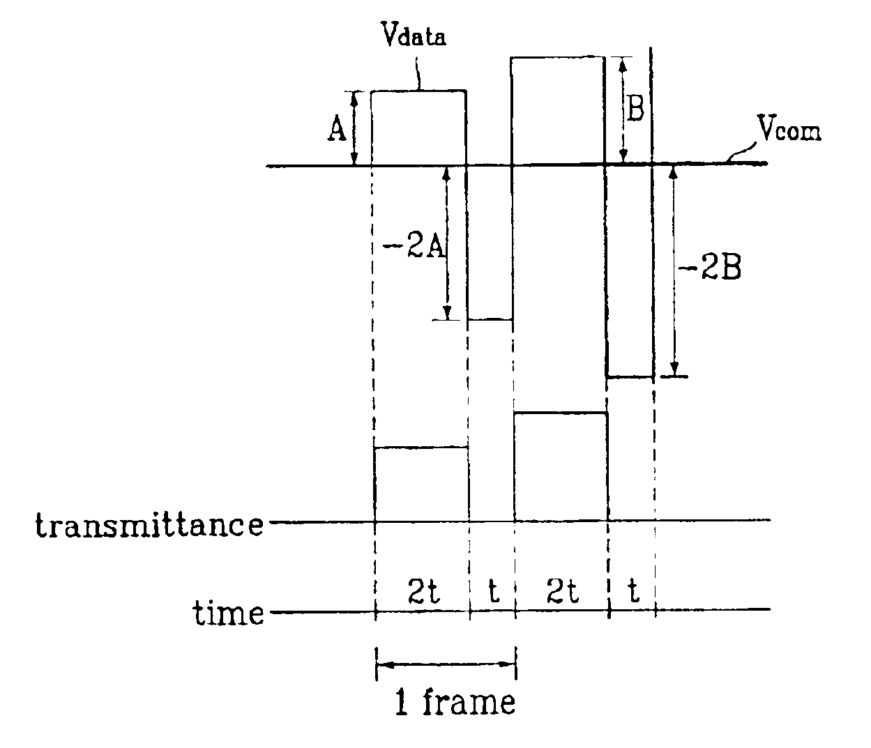
[0046]A first embodiment of the present invention, shown in FIG. 6, has a uniform common voltage Vcom (that is, it is fixed). Positive data voltages and negative compensation voltages are selectively and alternatingly applied to the data lines. For convenience, since both data voltages and compensation voltages are applied to the same line, those voltages are jointly represented by the line Vdata. As shown, the positive data voltage is applied for a longer period of time than the negative compensation voltage. This improves the overall brightness by increasing the time that each pixel transmits light. However, in each frame the integrated value of the applied positive data voltage over time (with reference to Vcom) is matched by the integrated value of an applied negative compensation voltage over time (again, with reference to Vcom), with the negative compensation voltage being applied for a shorter period of time. Thus, the magnitude of the negative compensation voltage is gr...

second embodiment

[0050

[0051]A second embodiment according to the present invention, illustrated in FIG. 7, uses a varying common voltage Vcom. In particular, as shown, the common voltage Vcom is greater when the (negative) compensation voltage is applied. Also as shown, the positive data voltages and the negative compensation voltages are applied in each frame. However, the positive data voltage is applied for a longer period of time in each frame than the negative compensation voltage. This improves overall brightness by enabling each pixel to transmit light for a greater period of time in each frame.

[0052]Specifically, scan voltages are applied to a plurality of gate lines that connect to the gate drive part. The scan voltages determine the ‘on / off state of the thin film transistors. The scan voltages are applied for predetermined portions of a predetermined frame period. When the scan voltages correspond to a high level, the thin film transistor is turned on.

[0053]The scan voltages are applied su...


PUM

PropertyMeasurementUnit
voltageaaaaaaaaaa
voltageaaaaaaaaaa
ferroelectricaaaaaaaaaa

Abstract

A method of driving a ferroelectric liquid crystal display with improved brightness while providing DC compensation. The method includes applying a data voltage, a compensation voltage, and a common voltage to each display pixel in each frame so as to selectively drive the liquid crystals, wherein the compensation voltage has a polarity (referenced to the common voltage) that is opposite the data voltage. The data voltage is applied for a longer period of time than the compensation voltage, but the magnitude of the compensation voltage is greater than the magnitude of the data voltage (when both are referred to the common voltage).

Description

[0001]This application claims the benefit of Korean Application No. P2001-63199, filed on Oct. 13, 2001, and which is hereby incorporated by reference.BACKGROUND OF THE INVENTION[0002]1. Field of the Invention[0003]The present invention relates to liquid crystal displays, and more particularly, to a method of driving ferroelectric liquid crystal displays with improved contrast and brightness.[0004]2. Discussion of the Related Art[0005]Recently, liquid crystal displays (hereinafter abbreviated LCDs), which are low power consuming, low volume flat panel displays, have been replacing conventional cathode ray tubes in many applications. Liquid crystals having both liquid fluidity and optical crystal properties. LCDs operate by varying arrangement of liquid crystal using applied electric fields.[0006]LCDs functionally include a liquid crystal panel and display drivers. The liquid crystal panel includes a lower (or array) substrate having pixel electrodes and thin film transistors arrange...

Claims


Application Information

Patent Timeline
Patent Type & Authority Patents(United States)
IPC IPC(8): G09G3/36G02F1/133G09G3/20
CPCG09G3/3651G09G3/2011G09G2310/06G09G2320/0204G02F1/133
Inventor CHOI, SU SEOK
Owner LG DISPLAY CO LTD
Why Eureka
Try Eureka