

Electrode structure for iontophoresis device and method of producing the same
- Summary
- Abstract
- Description
- Claims
- Application Information
AI Technical Summary
Benefits of technology
Problems solved by technology
Method used
Image

Examples
examples
[0065]Hereinafter, the electrode structure for the iontophoresis device of the invention and the method of producing the same will be described more particularly with reference to figures. At first, an example of the backing (Ia) of the electrode structure will be described below. (Examples 1 to 11 and comparative examples 1 to 4)
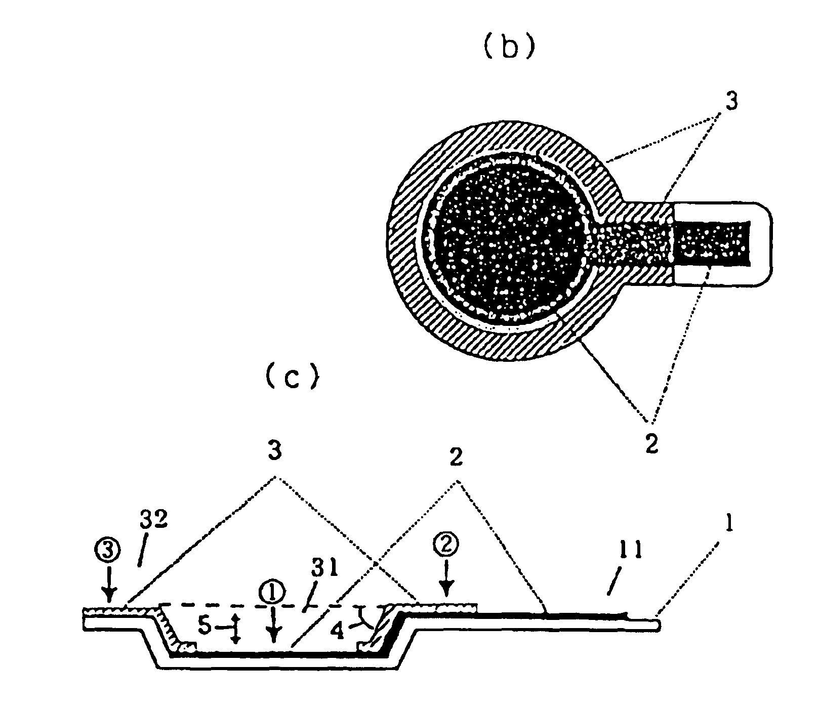
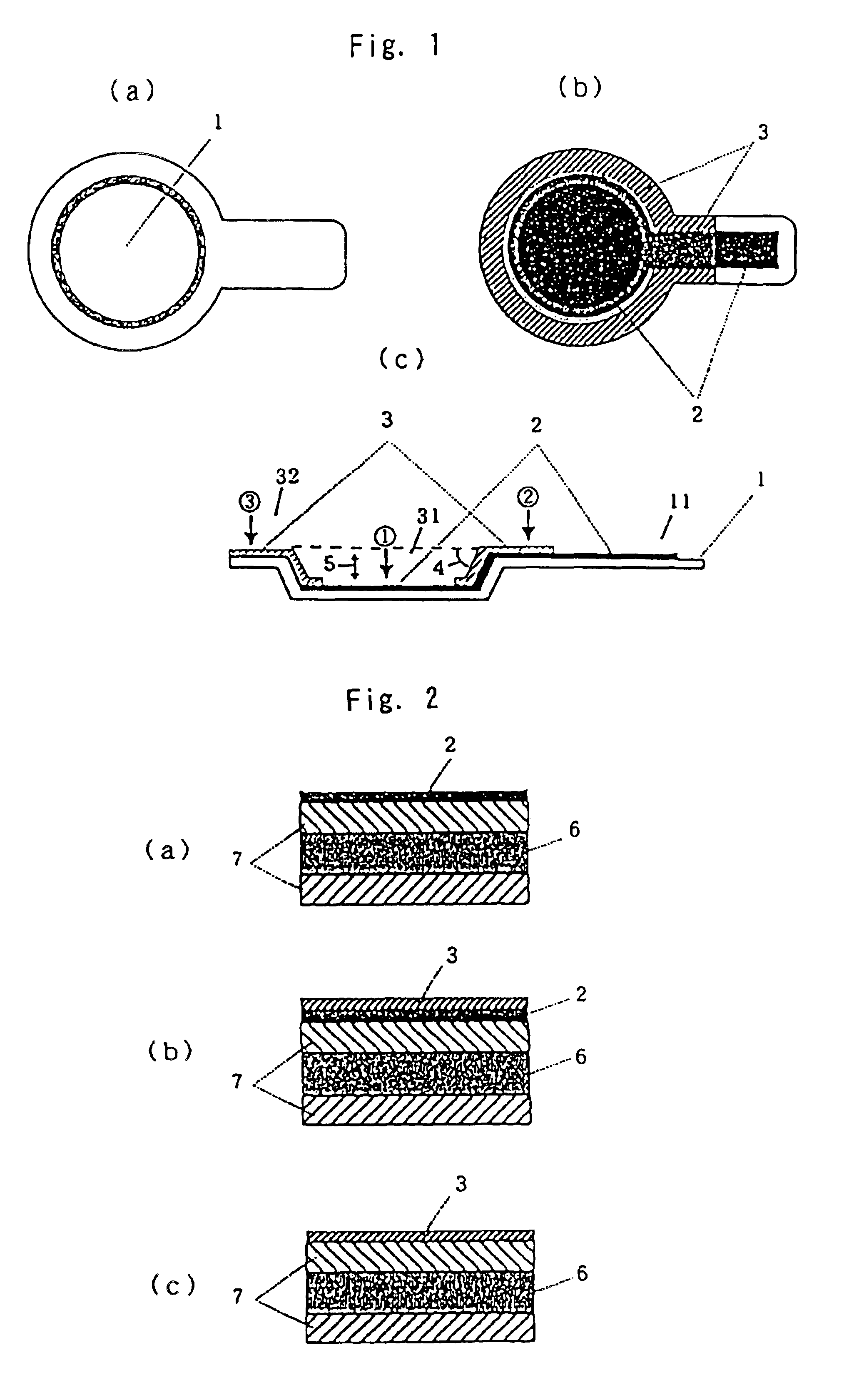
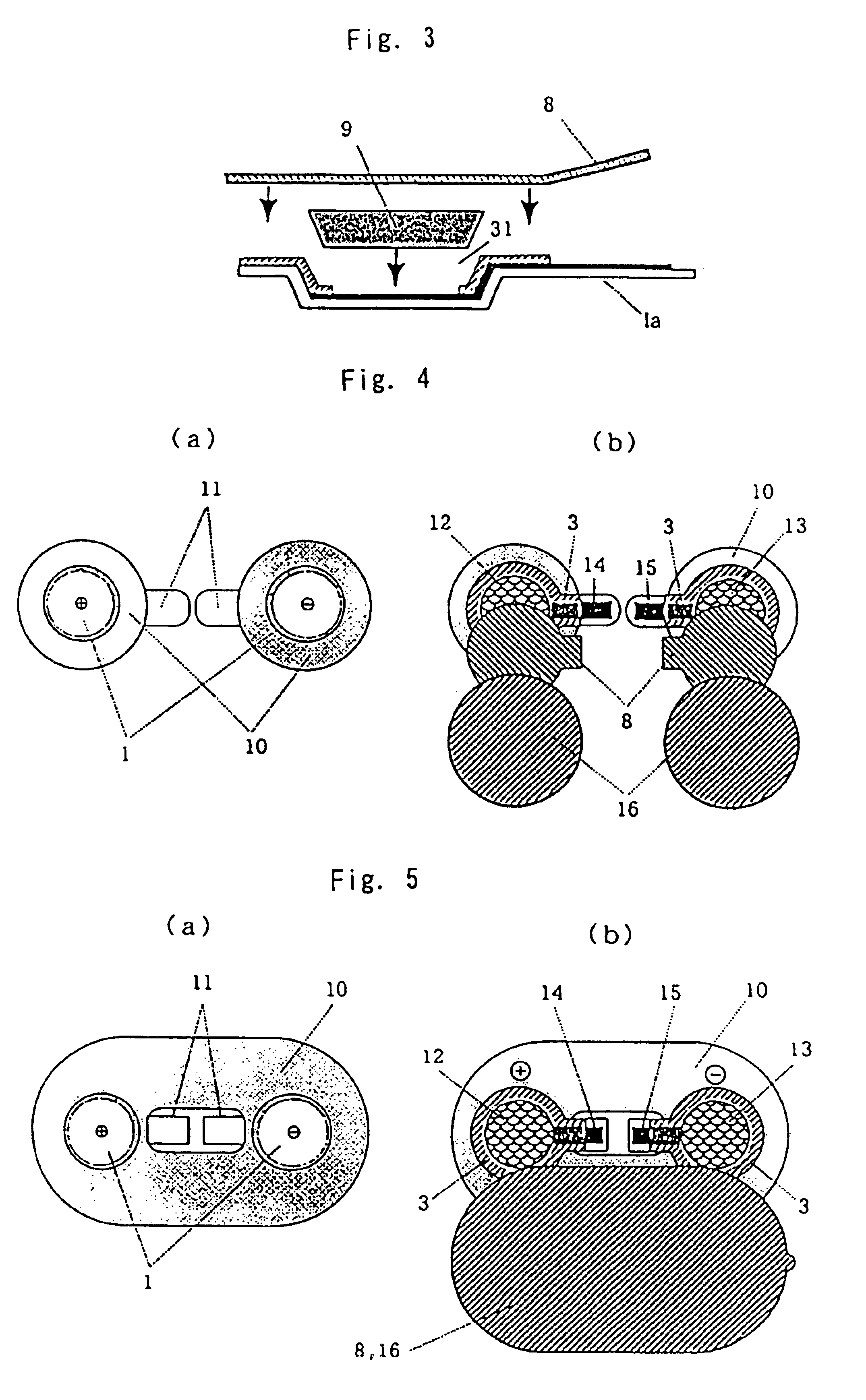
[0066]FIG. 1 shows an outlined figure of the backing (Ia) of the iontophoresis device according to the invention, (a) shows the front view, (b) shows the back side view, and (c) shows a cross-sectional view. FIG. 2 shows the substrate layer structure of the backing (Ia) of the iontophoresis device according to the invention, (a) shows section {circle around (1)} of FIG. 1 (c), (b) shows section {circle around (2)}, and (c) shows section {circle around (3)}. Further, FIG. 3 shows a schematic figure showing the basic embodiment of the electrode structure (Ib).
[0067]Regarding the manufacture of the backing (Ia) of the iontophoresis device of the invention, at ...
experiment 1
(Experiment 1)
[0073]Regarding the backing of the examples 1 to 11 and the comparative examples 1 to 4, the uniformity of the processed products, the flexibility of the backings to the skin, and the strength of the molding portions were sensuously evaluated. Incidentally the judgment standards are as follows.
[0074]Further if the processing temperature was high, since the effect was caused on the printed portions such as electrode layers, the total evaluation of the substrate films for the backings was performed while taking the processing temperature into consideration. The evaluation results are shown in Table 3.
[0075]Having high uniformity: ⊚, having not so high uniformity but no practical problem for use: ∘, having deformation in some portion and problematic for use: Δ, considerably shrunk and deformed and difficult to be used: ×.
[0076]No hardness and no unpleasant feeling: ⊚, slightly hard feeling but no unpleasant feeling: ∘, hard feeling and unpleasant feeling: Δ, hard and no f...
example 20
[0090]According to the manufacture process shown in the FIG. 7, FIG. 4 and FIG. 5 show the examples of the separation type electrode structure of which an anode and a cathode were independently produced in an iontophoresis device of the invention. As shown in the figures, an adhesive sheet 10 was formed in the front face of the substrate film 1. Further, an anode side conductive layer 12 was formed in the molding portion in the anode side and a cathode side conductive layer 13 was formed in the molding portion in the cathode side, respectively. An anode side electrode layer 14 and a cathode side electrode layer 15 were respectively led to lead portions 11 from inner bottom portions of respective molding portions and insulating layers 3 were formed in the outer circumferential portions of the respective molding portions. Cover members 8 were so disposed as to carrying out sealing between the insulating layers 3 and themselves. Liners 16 for adhesive sheets were put thereon. In the el...
PUM
 Abstract
Description
Claims
Application Information