Determining defects in OLED devices

Active Publication Date: 2005-07-12
GLOBAL OLED TECH
View PDF12 Cites 24 Cited by
  • Summary
  • Abstract
  • Description
  • Claims
  • Application Information

AI Technical Summary

Benefits of technology

[0009]It is therefore an object of the present invention to provide a detection arrangement that is particularly effective for determining defects in size, shape, location, and light intensity of pixels in one or more OLED devices.
[0014]The present invention provides the following advantages. It makes use of the property that the emissive layers of OLED devices can be excited by a illumination source using a predetermined portion of the spectrum and an image can be captured from the excited pixels of the OLED device. By operating on the converted digital image an effective defect detection arrangement can be achieved. The present invention can be configured to operate in a variety of environments, including operation within a vacuum or controlled atmosphere chamber.

Problems solved by technology

It has been difficult to achieve high resolution of pixel sizes using shadow masking.
Moreover, there are problems of alignment between the substrate and the shadow mask, and care must be taken that pixels are formed in the appropriate locations.
When it is desirable to increase the substrate size, it is difficult to manipulate the shadow mask to form appropriately positioned pixels.
A further disadvantage of the shadow-mask method is that the mask holes can become plugged with time.
Plugged holes on the mask lead to the undesirable result of non-functioning pixels on the EL display.

Method used


Image

  • Determining defects in OLED devices
  • Determining defects in OLED devices
  • Determining defects in OLED devices

Examples


Embodiment Construction

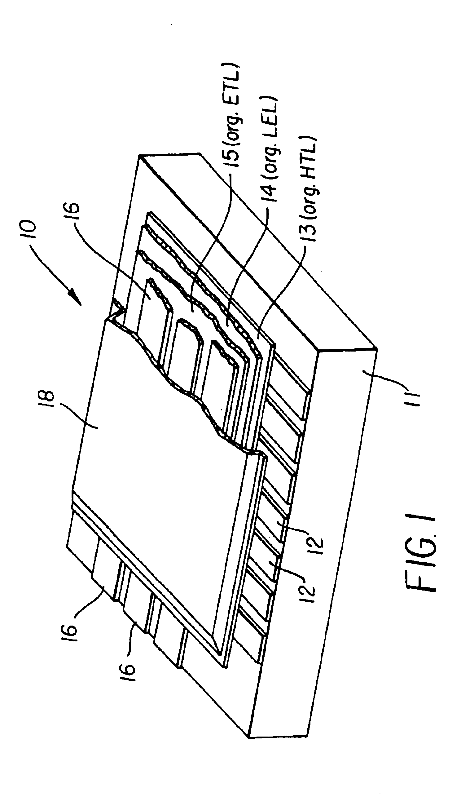
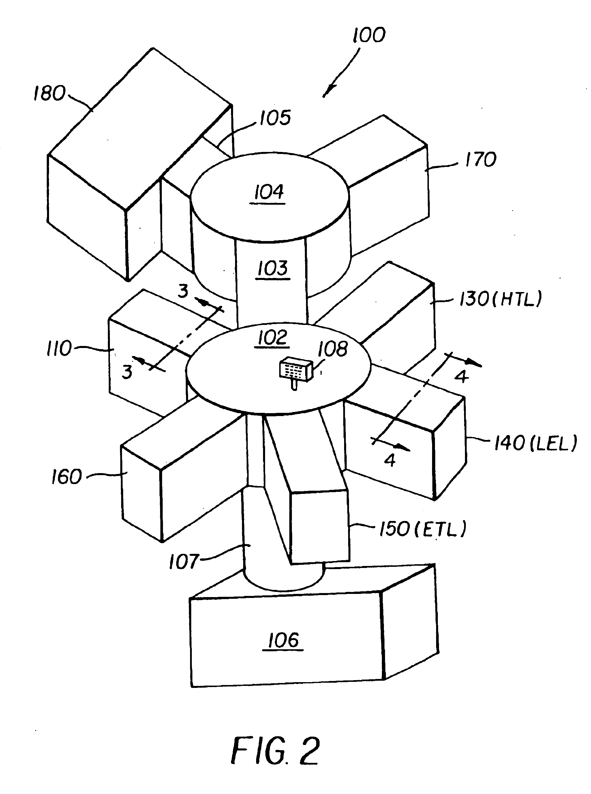
[0024]The inspection system described herein utilizes the phenomenon called photoluminescence. Photoluminescence is the process whereby a material absorbs light energy within a certain wavelength range, and re-emits that light energy at longer wavelengths. Phosphorescence and fluorescence are two separate emission pathways collectively termed photoluminescence. The absorbed light is called excitation light, and the resulting luminescent light is called emission light. The wavelengths of absorption and emission are dependent upon the specific composition of the material; in the case of the organic materials deposited in an OLED display, the emission wavelengths from photoluminescence are very similar to the wavelengths generated by electroluminescence, the underlying process for normal display usage. Because the excitation wavelengths depend upon the absorption characteristics of the material to be inspected, a predetermined portion of the spectrum can be chosen for best excitation. ...


PUM


Abstract

A method of determining defects in OLED devices having a plurality of pixels, each with its own emissive layer, which are capable of being excited by input light to produce an output color light response, including illuminating one or more OLED devices or a portion of an OLED device with light in a predetermined portion of the spectrum so that the pixel emissive layers are excited to produce an output color response for each pixel, capturing an image of the output light produced by the excited pixels and converting such captured light into a digital image; and determining device pixel size, shape, location, and emitted light intensity from the digital image and comparing such size, shape, location, and emitted light intensity with predetermined acceptable size, shape, location, and emitted light intensity ranges to determine whether there is a defect in the OLED device(s).

Description

FIELD OF THE INVENTION[0001]The present invention relates to organic light emitting devices (OLED) and more particularly to determining defects in such devices.BACKGROUND OF THE INVENTION[0002]An organic light-emitting device, also referred to as an organic electroluminescent device, can be constructed by sandwiching two or more organic layers between first and second electrodes.[0003]In a passive matrix organic light-emitting device of conventional construction, a plurality of laterally spaced light-transmissive anodes, for example indium-tin-oxide (ITO) anodes are formed as first electrodes on a light-transmissive substrate such as, for example, a glass substrate. Two or more organic layers are then formed successively by vapor deposition of respective organic materials from respective sources, within a chamber held at reduced pressure, typically less than 10−3 Torr. A plurality of laterally spaced cathodes are deposited as second electrodes over an uppermost one of the organic la...

Claims


Application Information

Patent Timeline
IPC IPC(8): H01J9/42H01T21/06H01T21/00H05B33/14H05B33/10H05B33/12H01L27/32H01L51/50H01L51/56
CPCH01L51/56H01L27/3281H01L2251/568H10K59/17H10K71/861H10K71/00
Inventor KALTENBACH, THOMAS F.GUIGUIZIAN, PAUL J.STEPHENSON, DONALD A.
Owner GLOBAL OLED TECH
Why Eureka
Try Eureka