Method for manufacturing a memory element

a memory element and manufacturing method technology, applied in the field of memory devices, can solve the problems of increasing the number of memory components, shrinking the memory devices, and reducing the access time of the memory devices

Inactive Publication Date: 2005-07-12
GLOBALFOUNDRIES INC
View PDF14 Cites 23 Cited by
  • Summary
  • Abstract
  • Description
  • Claims
  • Application Information

AI Technical Summary

Problems solved by technology

Shrinking the memory devices not only increases the number of memory components that can be manufactured from a single semiconductor wafer, but also decreases their access times.
Although these te

Method used


Image

  • Method for manufacturing a memory element
  • Method for manufacturing a memory element
  • Method for manufacturing a memory element

Examples


Embodiment Construction

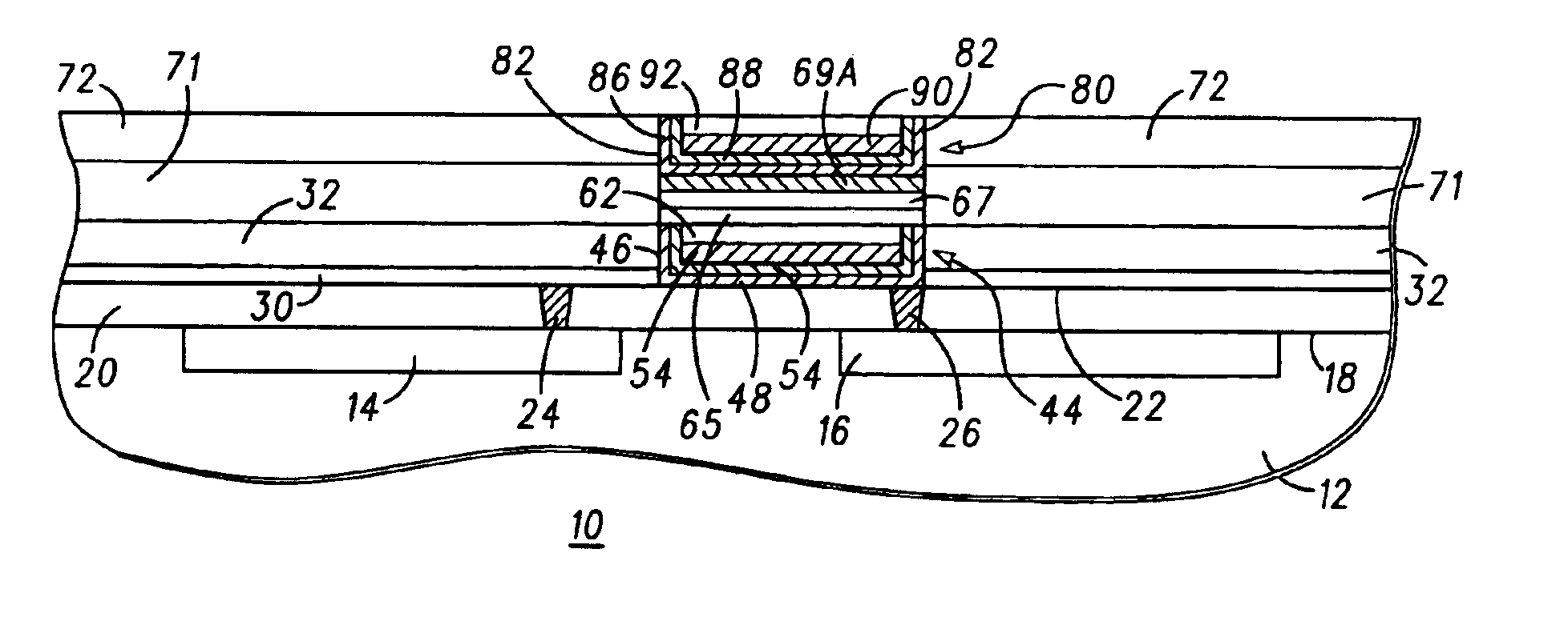
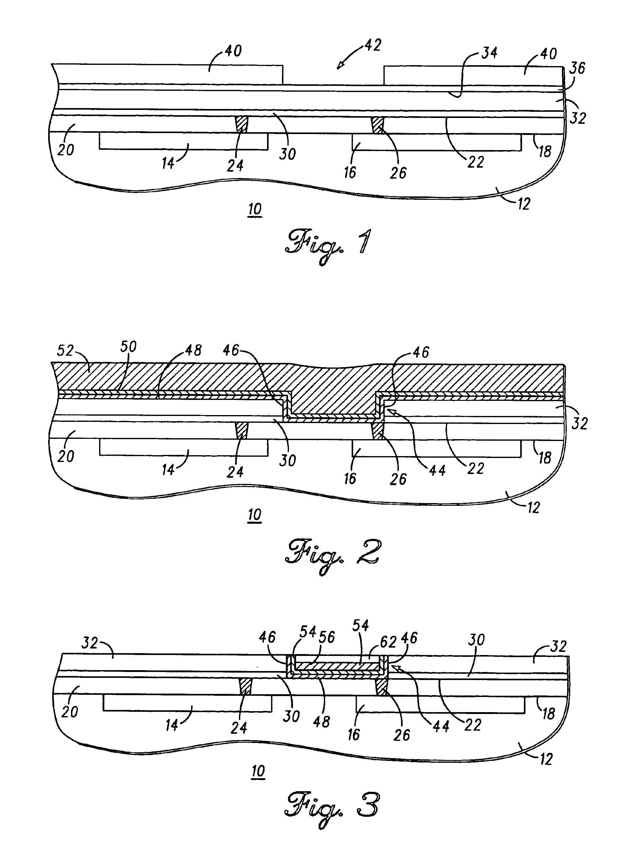
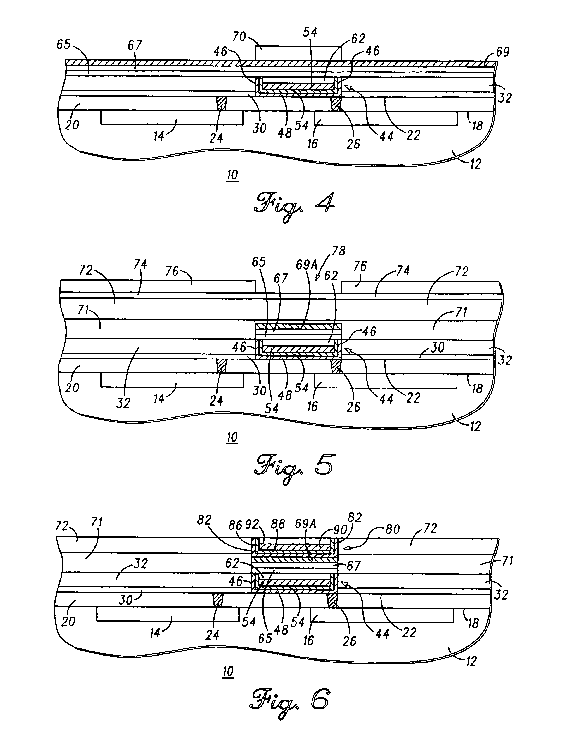
[0010]Generally, the present invention provides a method for manufacturing a memory device having a memory element comprising a sulfide of copper (CuxS, where x is greater than or equal to one and less than or equal to two, i.e., 1≦x≦2). In accordance with one embodiment, the memory device comprises a layer of copper sulfide formed by decomposing sulfur dioxide in a reaction chamber having a reducing ambient. In one aspect, the copper sulfide is formed on a copper electrode. The decomposition of the sulfur dioxide generates hydrogen sulfide that reacts with the copper electrode to form a sulfide of copper such as, for example, cuprous sulfide or cupric sulfide. After formation of the memory element, an electrode is coupled to the sulfide layer. An advantage of the present invention is that the formation of the sulfide layer can be readily integrated into semiconductor process flows. In accordance with another embodiment, a memory element comprising a sulfide of copper is coupled to ...


PUM


Abstract

A method for manufacturing the memory device by plasma decomposition of sulfur dioxide. A first copper electrode having a surface is provided. The surface of the first copper electrode may be made amorphous. A copper sulfide layer, CuxS, where 1≦x≦2, is disposed on the copper surface by decomposing sulfur dioxide in an ambient containing excess hydrogen. The copper sulfide layer may be is cuprous sulfide or cupric sulfide. A second copper electrode is coupled to the copper sulfide layer.

Description

FIELD OF THE INVENTION[0001]The present invention relates, in general, to memory devices and, more particularly, to memory devices that include sulfide based memory elements.BACKGROUND OF THE INVENTION[0002]Semiconductor component manufacturers are constantly striving to decrease the cost of manufacturing their products. One technique for reducing cost has been to shrink or reduce the lateral dimensions of the devices that make up the semiconductor components. In addition to shrinking the lateral dimensions, devices have been made even smaller by stacking metal interconnect layers that route signals to the various devices in the semiconductor component. The combination of shrinking and stacking has allowed manufacturers to increase the number of semiconductor components that can be manufactured from a single semiconductor wafer. These techniques have been especially beneficial for manufacturers of memory devices because these types of semiconductor components are formed as arrays th...

Claims


Application Information

Patent Timeline
IPC IPC(8): H01L21/70H01L21/8238H01L45/00
CPCH01L45/04H01L45/1633H01L45/142H01L45/1233H10N70/20H10N70/8822H10N70/028H10N70/826
Inventor BUYNOSKI, MATTHEW S.
Owner GLOBALFOUNDRIES INC
Why Eureka
Try Eureka