Radiation detector and method of manufacture thereof

a technology of radiation detector and manufacturing method, which is applied in the direction of optical radiation measurement, mechanical vibration separation, instruments, etc., can solve the problems of reducing the output and resolution of end portions, and it is difficult to achieve large imaging area, so as to facilitate thinning the detector, facilitate the manufacturing of substrates, and increase the effect of effective light-receiving portions

Inactive Publication Date: 2005-07-19
HAMAMATSU PHOTONICS KK
View PDF32 Cites 36 Cited by
  • Summary
  • Abstract
  • Description
  • Claims
  • Application Information

AI Technical Summary

Benefits of technology

[0005]It is an object of the present invention to provide a radiation detector which can attain both a small, thin structure and a large imaging area, and can be easily manufactured, and manufacturing method thereof.
[0008]That is, the radiation detector according to the present invention is manufactured by forming the scintillator on the surface of the light-receiving portion of the solid-state imaging element by vapor deposition such as vapor deposition after the solid-state imaging element is fixed on the support surface of the substrate. In this case, the holding portions of the substrate are used to project the surface of the light-receiving portion toward the vapor deposition chamber. Hence, no projecting portion which becomes an obstacle is formed on the light-receiving portion in forming the scintillator, thereby uniformly forming the scintillator on the entire light-receiving portion. This can ensure the resolution in a peripheral region and attain the large area of the effective light-receiving portion. The FOP is not used, thus facilitating thinning the detector.
[0009]These holding portions may be tab-shaped to conform to the side wall of the substrate, or the upper surfaces of these holding portions may be continuously flush with the support surface. This facilitates manufacturing the substrate and mounting the solid-state imaging element on the substrate.

Problems solved by technology

However, when a light-receiving portion is formed on the entire light-receiving surface, it is difficult to uniformly form the scintillator on the entire light-receiving portion, thus decreasing the output and resolution of end portions.
This makes it difficult to attain the large imaging area.

Method used


Image

  • Radiation detector and method of manufacture thereof
  • Radiation detector and method of manufacture thereof
  • Radiation detector and method of manufacture thereof

Examples


Embodiment Construction

[0020]Preferred embodiments of the present invention will be described in detail below with reference to the accompanying drawings. To facilitate the comprehension of the explanation, the same reference numerals denote the same parts, where possible, throughout the drawings, and a repeated explanation will be omitted. The size and shape of each drawing need not always be the same as the actual design. Some parts are exaggerated for convenience of understanding.

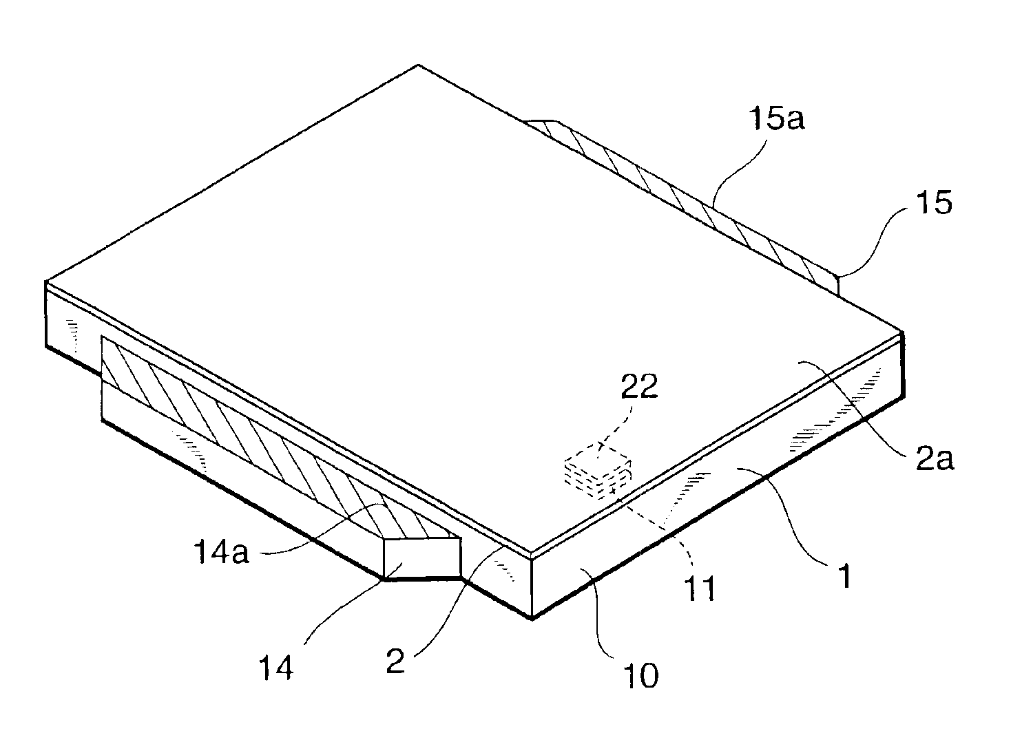
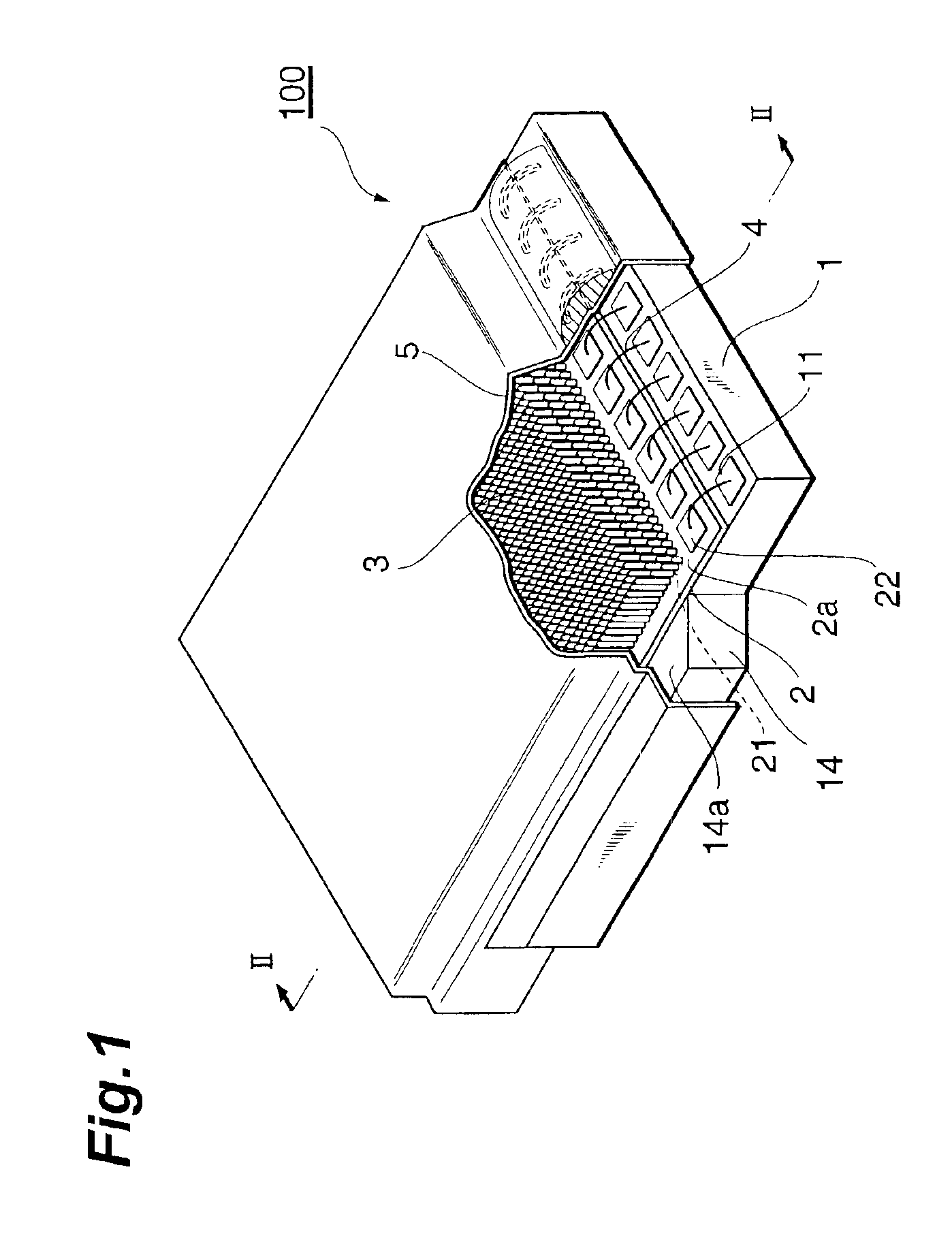
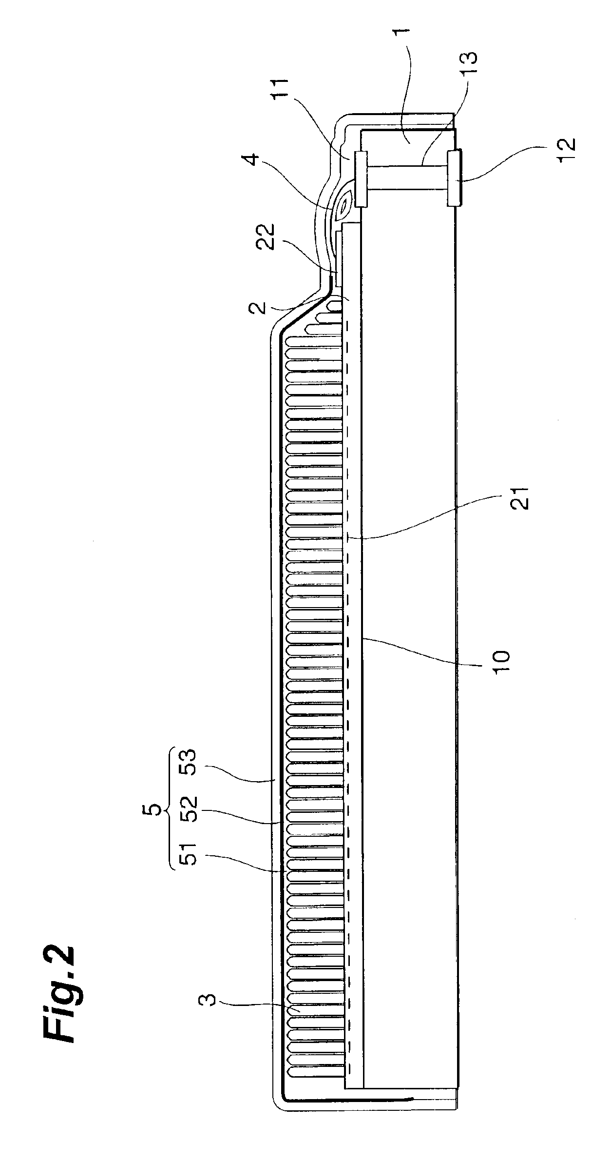
[0021]FIG. 1 is a perspective view showing an embodiment of a radiation detector according to the present invention, and FIG. 2 is a sectional view thereof. A radiation detector 100 of this embodiment is constituted by mounting a solid-state imaging element 2 on a ceramic substrate 1. The substrate 1 has in the center of the upper surface a support surface 10 where the solid-state imaging element 2 is set. A plurality of electrode pads 11 are arrayed along one side of the support surface 10. These electrode pads 11 are electri...


PUM

PropertyMeasurementUnit
timeaaaaaaaaaa
thicknessaaaaaaaaaa
thicknessaaaaaaaaaa

Abstract

A solid-state imaging element 2 having a light-receiving portion where a plurality of photoelectric conversion elements 21 are arranged, and electrode pads 22 electrically connected to the photoelectric conversion elements 21 is mounted on a substrate 1. A scintillator 3 is formed on the surface of the light-receiving portion of the solid-state imaging element. Around a support surface 10 where the solid-state imaging element 2 of the substrate 1 is mounted, holding portions 14 and 15 are formed on opposing side walls to hold and project the surface of the light-receiving portion from a vapor deposition holder toward a vapor deposition chamber in forming the scintillator 3.

Description

TECHNICAL FIELD[0001]The present invention relates to a radiation detector used for radiation imaging and a manufacturing method thereof and, more particularly, to a compact dental radiation detector used upon insertion into an oral cavity and a manufacturing method thereof.BACKGROUND ART[0002]X-ray image sensors using a CCD instead of an X-ray sensitive film are becoming popular as a medical X-ray diagnostic apparatus. In such a radiation imaging system, a radiation detection device having a plurality of pixels acquires two-dimensional image data by radiation as an electrical signal, and this signal is processed by a processor and displayed on a monitor.[0003]As a dental radiation detector used upon insertion into an oral cavity, a radiation detector which is disclosed in JP 10-282243 A has been known. In this radiation detector, an FOP (Fiber Optical Plate) with a scintillator is stuck on the light-receiving surface of a CCD. The radiation detector has a mechanism to convert incid...

Claims


Application Information

Patent Timeline
Patent Type & Authority Patents(United States)
IPC IPC(8): C23C14/50G01T1/20G01T7/00G01T1/24G01T1/00H01L27/14H01L31/09H01L31/08H04N5/32
CPCH01L27/14618H01L27/14663H01L2224/05554H01L2224/48091H01L2224/48227H01L2924/00014
Inventor HOMME, TAKUYAMIYAGUCHI, KAZUHISATAKABAYASHI, TOSHIO
Owner HAMAMATSU PHOTONICS KK
Why Eureka
Try Eureka