Method for bonding IC chips to substrates incorporating dummy bumps and non-conductive adhesive and structures formed

a technology of ic chips and substrates, which is applied in the direction of printed circuit assembling, printed circuit stress/warp reduction, printed circuit board manufacturing, etc., can solve the problems of premature failure of solder connections, mismatch of thermal expansion coefficients between printed circuit boards and silicon chips, and time-consuming task of filling gaps between silicon chips and substrates

Inactive Publication Date: 2005-07-19
IND TECH RES INST
View PDF4 Cites 66 Cited by
  • Summary
  • Abstract
  • Description
  • Claims
  • Application Information

AI Technical Summary

Problems solved by technology

The use of organic substrates, or polymeric-base substrates, in printed circuit boards, flexible substrates or interposers introduces a new source of problem for the flip-chip bonding of a silicon chip which is mostly inorganic to such substrates.
The problem is the mismatch of coefficients of thermal expansion (CTE) between the printed circuit board and the silicon chip.
The extreme mismatch in CTE's between the silicon chip and the organic substrate of the printed circuit board therefore subjects solder joints formed therein between to extremely large thermal strains, which leads to premature failure of the solder connections.
While the introduction of the underfill layer between

Method used


Image

  • Method for bonding IC chips to substrates incorporating dummy bumps and non-conductive adhesive and structures formed
  • Method for bonding IC chips to substrates incorporating dummy bumps and non-conductive adhesive and structures formed
  • Method for bonding IC chips to substrates incorporating dummy bumps and non-conductive adhesive and structures formed

Examples


Embodiment Construction

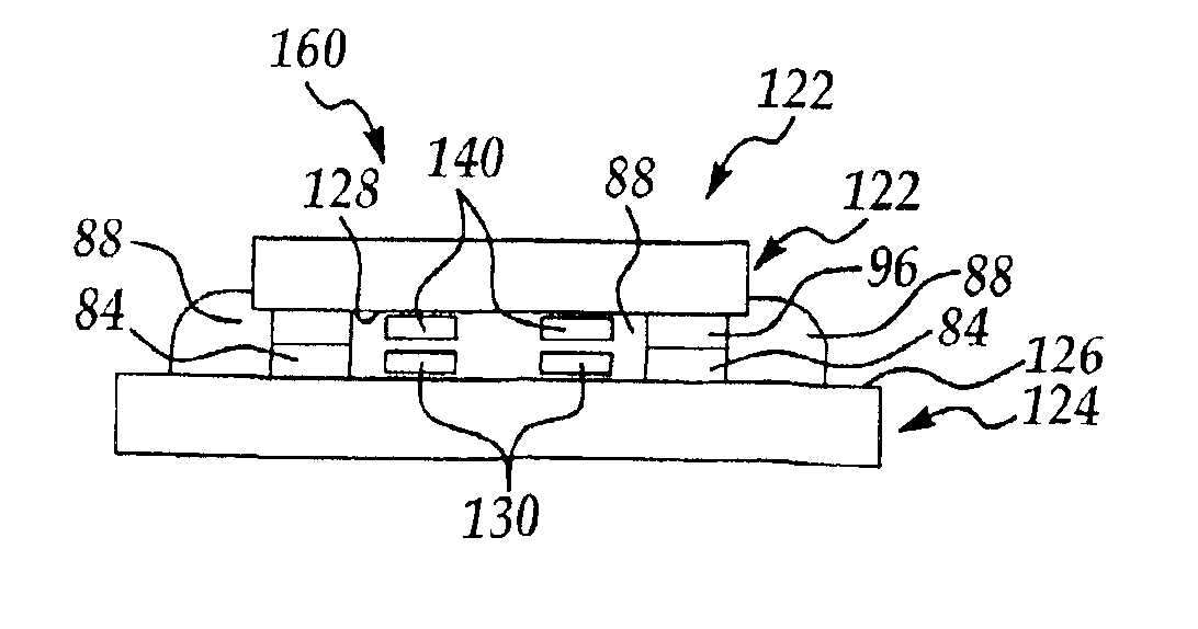
[0053]The present invention discloses an IC chip / substrate assembly bonded together by a non-conductive adhesive and a method for forming the IC chip / substrate assembly.

[0054]The IC chip / substrate assembly is formed by an IC chip, a substrate and a non-conductive adhesive disposed therein between. The IC chip has bumps formed on an active surface, wherein the bumps may be formed of Au, Ni, or Sn-containing (solder-type) alloys.

[0055]The substrate has a plurality of bond pads formed on a top surface. The plurality of bond pads may be formed of copper, aluminum or any other suitable metal.

[0056]While the present invention method for bonding an IC chip to a substrate can be used in any semiconductor assembly applications, it is particularly suitable for bonding an IC chip which is a driver chip for a LCD display panel to a flexible substrate.

[0057]Referring now to FIG. 7A, wherein a present invention IC chip / substrate assembly 120 formed by an IC Chip 122 and a substrate 124 is shown. ...


PUM


Abstract

An IC chip/substrate assembly bonded together by a non-conductive adhesive and a method for forming the assembly. The assembly consists of an IC chip that has bumps formed on an active surface, a substrate that has bond pads formed on a top surface, wherein at least one of the IC chip and the substrate has dummy bumps formed in-between the bumps or the bond pads, and a non-conductive adhesive disposed in between and bonding the IC chip and the substrate together in a face-to-face relationship with the bumps in electrical communication with the bond pads.

Description

FIELD OF THE INVENTION[0001]The present invention generally relates to a method for forming IC chip / substrate assemblies incorporating dummy bumps and an adhesive and assemblies formed, more particularly, relates to a method for bonding an IC chip to a substrate by a non-conductive adhesive wherein at least one of the IC chip and substrate is formed with dummy bumps on a surface to be bonded and assemblies formed by the method.BACKGROUND OF THE INVENTION[0002]In the fabrication of modern semiconductor devices, the ever increasing device density and decreasing device dimensions demand more stringent requirements in the packaging or interconnecting techniques of the devices. In recent years, a flip-chip attachment method or flip-chip direct chip attachment (DCA) method has been used in packaging integrated circuit chips. In the flip-chip attachment method, instead of attaching an integrated circuit lead frame in a package, an array of solder balls is formed on the surface of the die f...

Claims


Application Information

Patent Timeline
IPC IPC(8): H01L21/56H01L21/02H05K1/02H05K3/30
CPCH01L21/563H01L24/27H01L24/29H01L2924/07802H01L2924/10253H01L2224/2919H01L2224/29111H01L2924/0132H01L2924/01033H01L2924/01006H05K3/305H05K1/0271H01L2924/3511H01L2224/16225H01L2224/73203H01L2224/73204H01L2224/83102H01L2224/83192H01L2224/92125H01L2924/01013H01L2924/01027H01L2924/01029H01L2924/0105H01L2924/01079H01L2924/01082H01L2924/09701H01L2924/14H01L2224/13111H01L2924/00015H01L2924/00014H01L2924/00H01L2224/05573H01L2224/05568H01L2224/05599
Inventor HSIEH, YU-TECHANG, SHYH-MINGLIN, WEN-TI
Owner IND TECH RES INST
Why Eureka
Try Eureka