Compact SRAM cell with FinFET

a technology of finfets and sram cells, applied in the field of transistors, can solve the problems of reducing the ability of the gate of the same to control whether, and the problems of the conventional mosfets suffering from several problems, and achieve the effect of reducing the distance between the two devices

Inactive Publication Date: 2005-08-02
TAIWAN SEMICON MFG CO LTD
View PDF14 Cites 180 Cited by
  • Summary
  • Abstract
  • Description
  • Claims
  • Application Information

AI Technical Summary

Benefits of technology

[0006]A method and system is disclosed for an SRAM device cell having at least one device of a first semiconductor type and at lease one device of a second semiconductor type. The cell has a first device of the first type constructed as a part of a first FinFET having one or more devices of the first type, a first device of the second type whose poly region is an extension of a poly region of the first device of the first type with no contact needed to connect therebetween, wherein the two devices are constructed using a silicon-on-insulator (SOI) technology so that they are separated by an insulator region therebetween so as to minimize the distance between the two devices.

Problems solved by technology

As MOSFETs are scaled to channel lengths below 100 nm, conventional MOSFETs suffer from several problems.
In particular, interactions between the source and drain of the MOSFET degrade the ability of the gate of the same to control whether the device is on or off.

Method used


Image

  • Compact SRAM cell with FinFET
  • Compact SRAM cell with FinFET
  • Compact SRAM cell with FinFET

Examples


Embodiment Construction

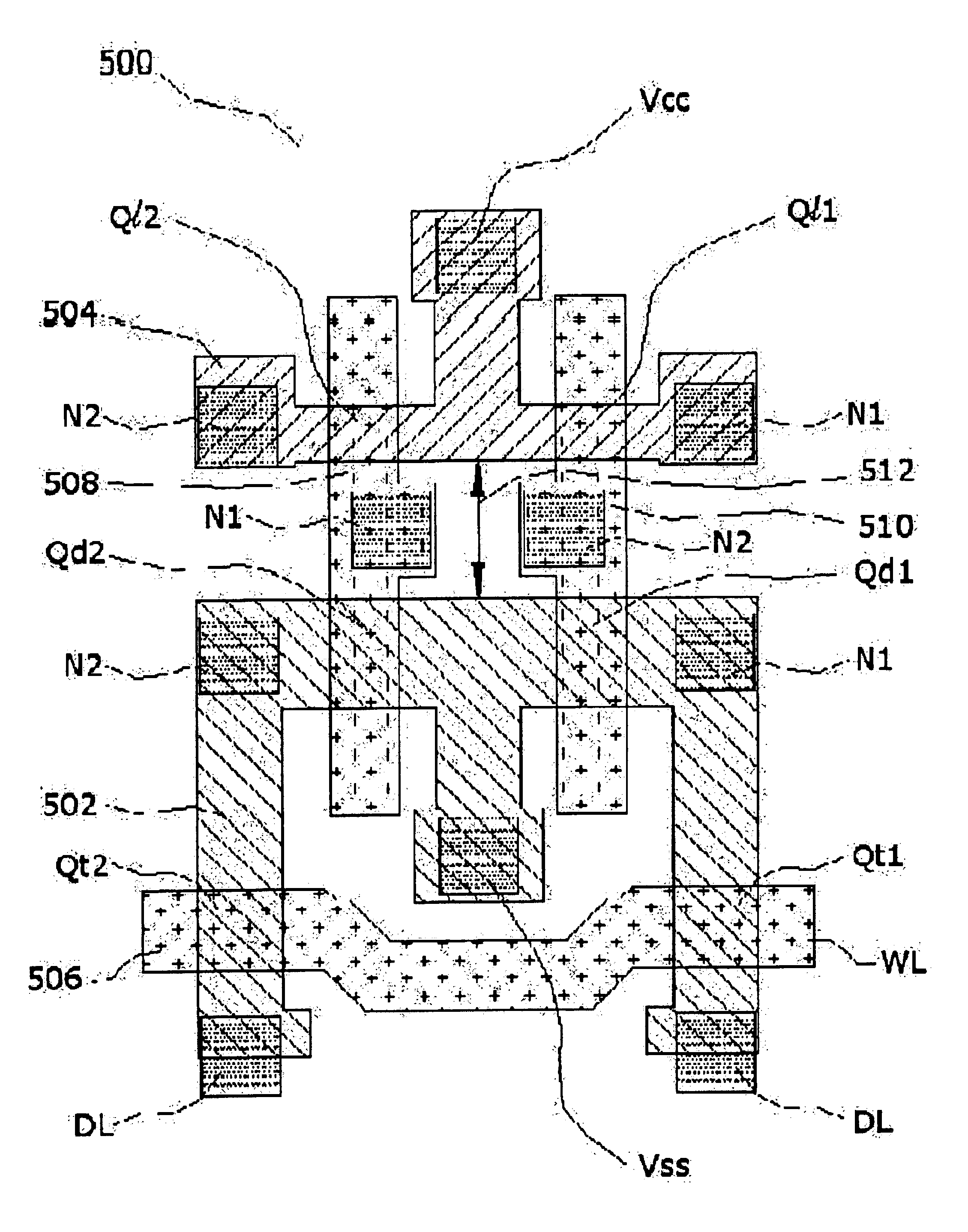
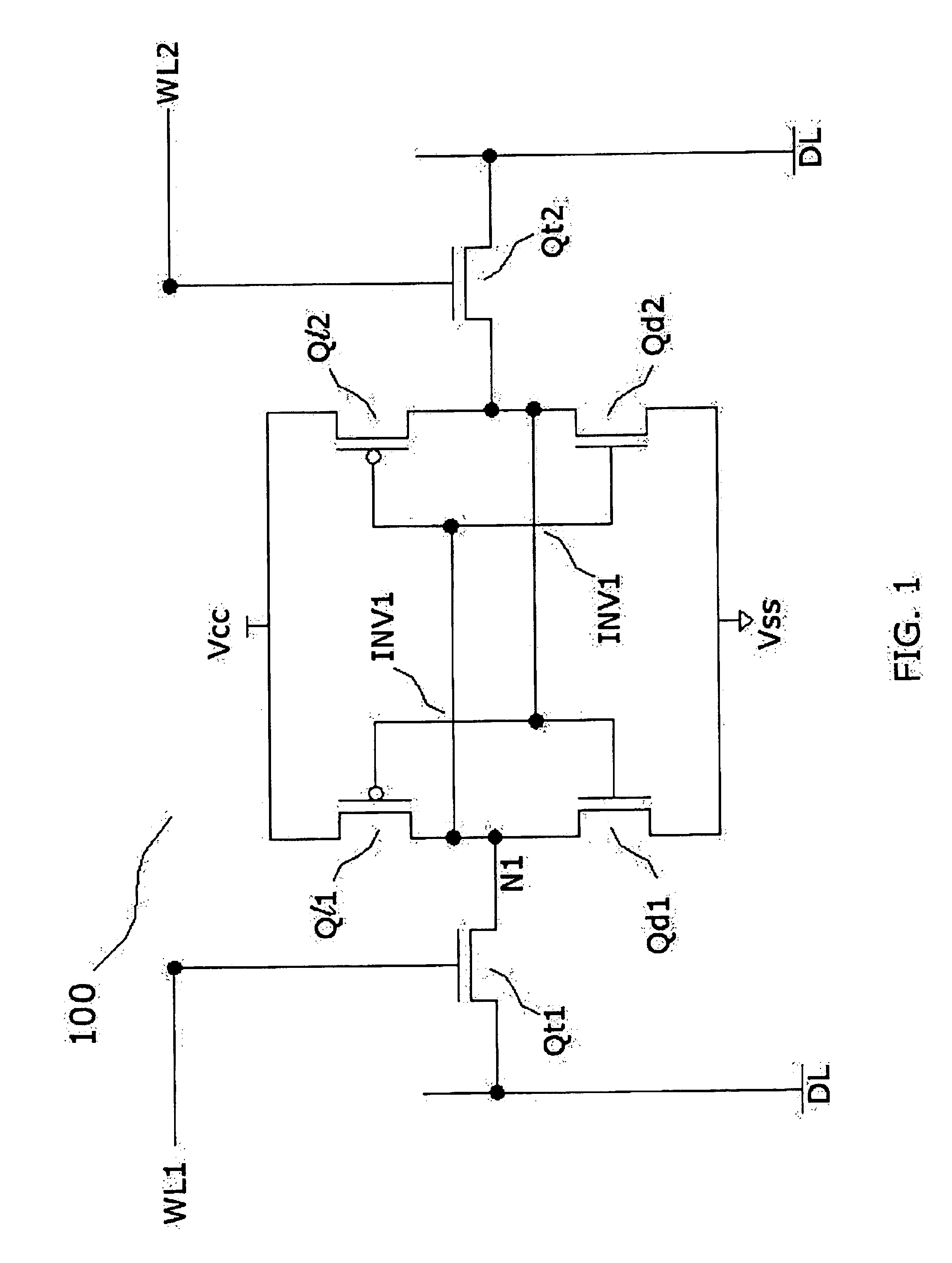
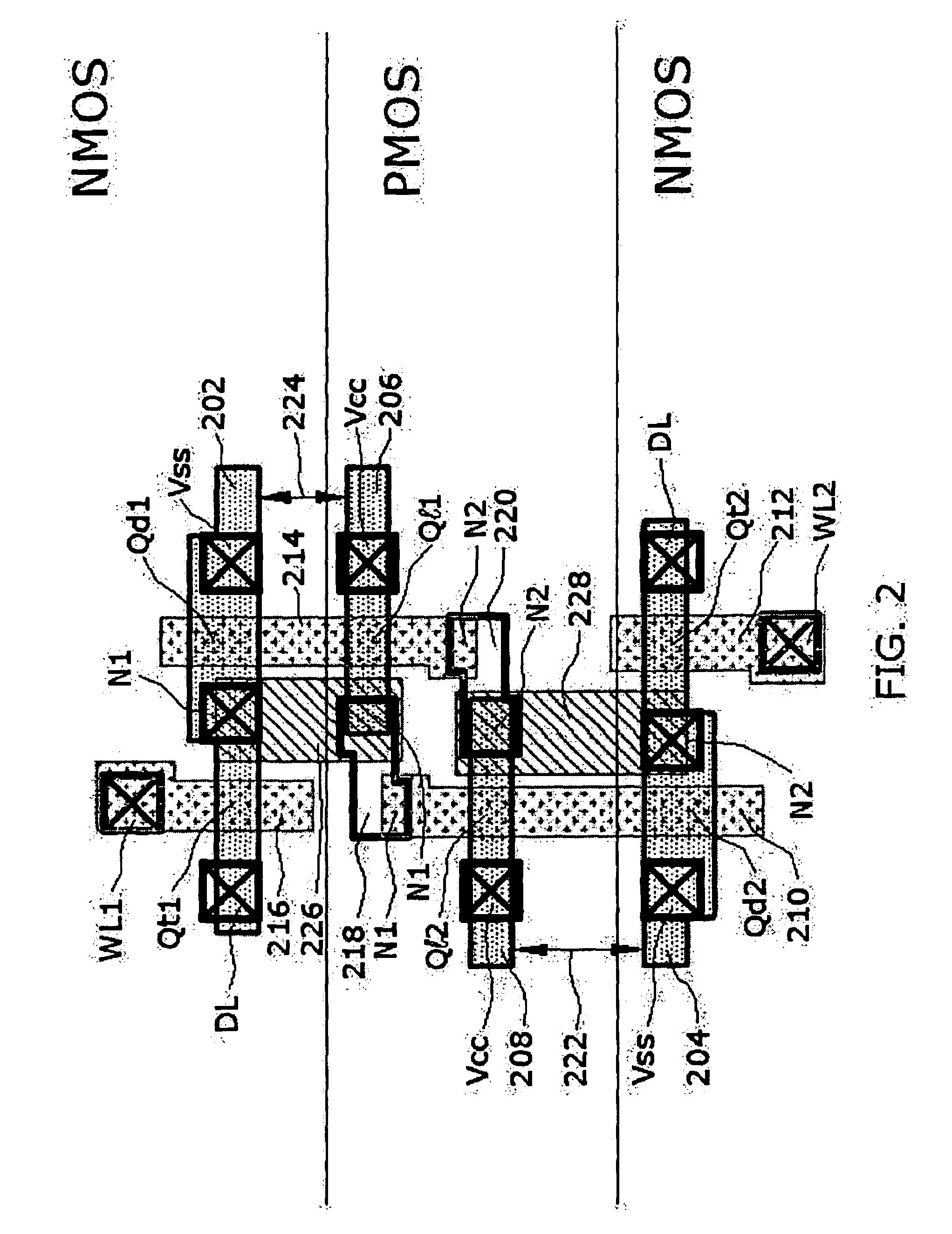
[0013]Silicon-on-insulator (SOI) MOSFETs are formed with an insulator (usually, but not limited to, silicon dioxide) below the device active region, unlike conventional “bulk” MOSFETs, which are formed directly on silicon substrates, and hence have silicon below the active region SOI is advantageous since it reduces unwanted coupling between the source and the drain of the MOSFET through the region below the channel. This is often achieved by ensuring that all the silicon in the MOSFET channel region can be either inverted or depleted by the gate (called a fully depleted SOI MOSFET). As device size is scaled, however, this becomes increasingly difficult, since the distance between the source and drain is reduced, and hence, increasing the interaction with the channel, reducing gate control and increasing short channel effects. SOI is also advantageous since it reduces unwanted coupling between the source and the drain of the adjacent MOSFET through the region of the well below STI / L...


PUM


Abstract

A method and system is disclosed for an SRAM device cell having at least one device of a first semiconductor type and at lease one device of a second semiconductor type. The cell has a first device of the first type constructed as a part of a first FinFET having one or more devices of the first type, a first device of the second type whose poly region is an extension of a poly region of the first device of the first type with no contact needed to connect therebetween, wherein the two devices are constructed using a silicon-on-insulator (SOI) technology so that they are separated by an insulator region therebetween so as to minimize the distance between the two devices.

Description

BACKGROUND OF THE DISCLOSURE[0001]This invention relates generally to transistors, and more particularly, to a compact memory transistor cell.[0002]Metal-oxide-Semiconductor field effect transistor (MOSFET) technology is the dominant electronic device technology in use today. Performance enhancement between generations of devices is generally achieved by reducing the size of the device, resulting in an enhancement in device speed. This is generally referred to as device “scaling”. As MOSFETs are scaled to channel lengths below 100 nm, conventional MOSFETs suffer from several problems. In particular, interactions between the source and drain of the MOSFET degrade the ability of the gate of the same to control whether the device is on or off. This phenomenon is called the “short-channel effect” (SCE).[0003]A conventional SRAM cell is comprised of first and second driver transistors whose drain-source paths are respectively connected between first and second storage nodes and ground, f...

Claims


Application Information

Patent Timeline
Patent Type & Authority Patents(United States)
IPC IPC(8): H01L27/148H01L27/11G11C11/412H01L21/336H01L21/8244H01L29/786
CPCG11C11/412H01L27/11H01L27/1104H01L29/66795H01L29/785Y10S257/903Y10S257/904H10B10/00H10B10/12
Inventor WANG, PING-WEIYANG, CHANG-TA
Owner TAIWAN SEMICON MFG CO LTD
Why Eureka
Try Eureka