Memory device with discrete layers of phase change memory material

a memory device and phase change technology, applied in the field of phase change memory devices, can solve the problems of slow reading and programming, large power consumption, and increasing the difficulty of cell scaling down to smaller sizes, and achieve the effect of reliable and repeated programmability

Inactive Publication Date: 2005-08-09
SILICON STORAGE TECHNOLOGY
View PDF4 Cites 334 Cited by
  • Summary
  • Abstract
  • Description
  • Claims
  • Application Information

AI Technical Summary

Benefits of technology

[0011]The present invention solves the aforementioned problems by the discovery that discrete layers of phase change memory material, that are separated by lattice mismatch interface materials, produce quantized resistivities that are more reliably and more repeatedly programmable.

Problems solved by technology

However, EEPROM memory cells are getting more difficult to scale down to smaller sizes, are relatively slow to read and program, and can consume a relatively large amount of power.
These patents recognize that the resistance of the memory material may drift, possibly outside a selected margin of error, which would result in a loss of stored data.
It can be difficult to accurately and repeatedly program multi-bit phase change memory cells with the desired degree of crystallization, to produce the desired resistance value(s).
On a microscopic scale, the properties of phase change material can be difficult to control and anticipate, especially if there is any resistance drift.

Method used


Image

  • Memory device with discrete layers of phase change memory material
  • Memory device with discrete layers of phase change memory material
  • Memory device with discrete layers of phase change memory material

Examples


Embodiment Construction

[0028]The present invention is an improved, programmable, memory material and a method of making such material, as well as devices that utilize such memory material. The programmable memory material of the present invention includes discrete layers of phase change material, separated by conductive interface layers, that produce quantized levels of resistivity.

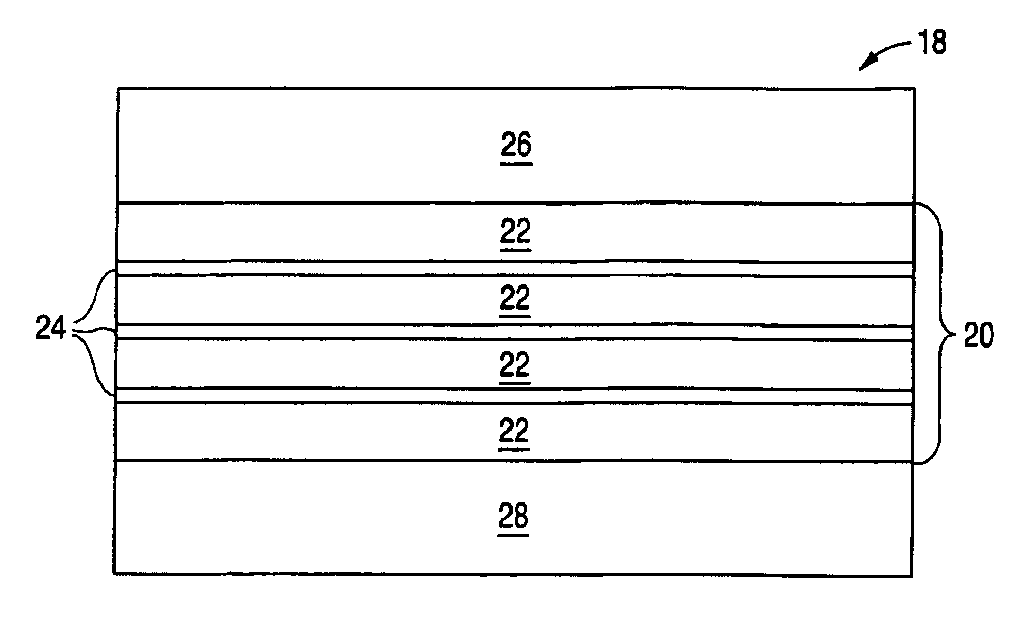
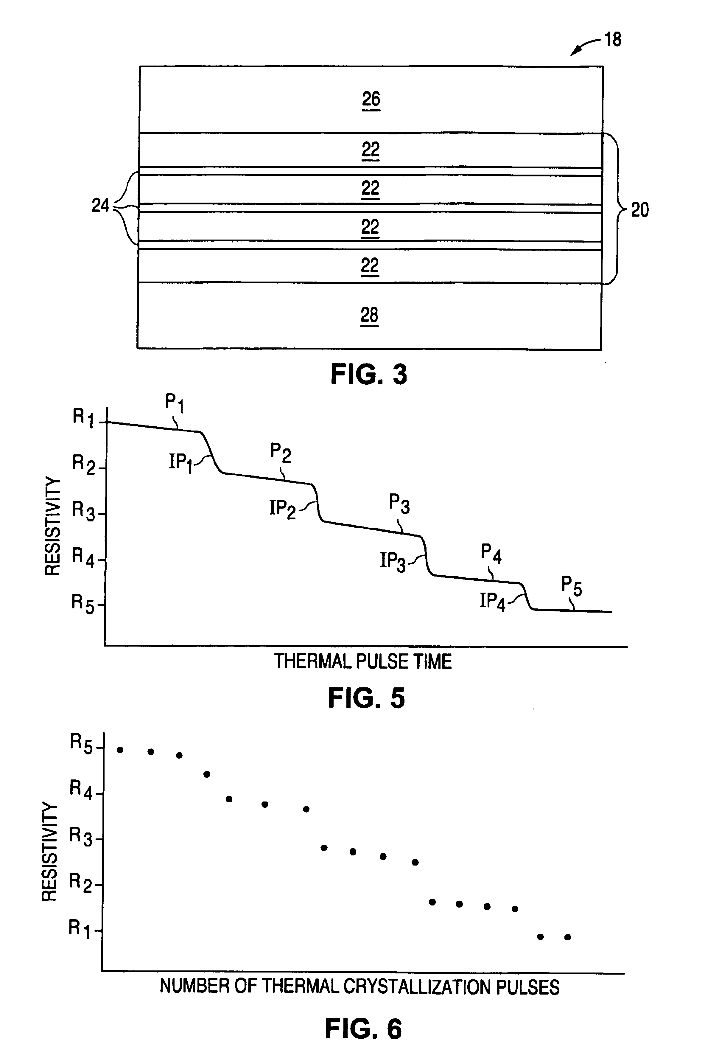
[0029]FIG. 3 illustrates a basic memory device 18 using programmable memory material 20 of the present invention. The memory material 20 includes a plurality of discrete layers 22 of phase change material, interlaced with a plurality of discrete layers 24 of lattice mismatch interface material. For illustration purposes only, four phase change material layers 22 (e.g. 0.3 to 100 nm thick), separated by three interface layers 24 (e.g. 0.2 to 0.8 nm thick) are shown in FIG. 3, however fewer or greater numbers of layers 22 / 24 with different thicknesses can be used. Ideally, the number of phase change material layers 22 corresponds...


PUM


Abstract

A phase changing memory device, and method of making the same, that includes programmable memory material disposed between a pair of electrodes. The programmable memory material includes discrete layers of phase change material, separated by conductive interface layers, that exhibits relatively stable resistivity values over discrete ranges of crystallizing and amorphousizing thermal pulses applied thereto, for multi-bit storage. The memory material and one of the electrodes can be disposed along spacer material surfaces to form an electrical current path that narrows in width as the current path approaches the other electrode, such that electrical current passing through the current path generates heat for heating the memory material disposed between the electrodes.

Description

FIELD OF THE INVENTION[0001]The present invention relates to phase change memory devices, and more particularly to phase change memory devices employing discrete and separated layers of phase change material.BACKGROUND OF THE INVENTION[0002]There are many types of computer memory technologies that are presently used to store computer programs and data, including dynamic random access memory (DRAM), static random access memory (SRAM), erasable programmable read-only memory (EPROM), and electrically erasable programmable read only memory (EEPROM), etc. Some memory technologies require electrical power to maintain the stored data (i.e. volatile memory), while others do not (i.e. non-volatile memory). Memory technologies can be read only, write once only, or repeatedly read / write.[0003]There is an increasing demand for repeatedly read / write, non-volatile memory. The primary non-volatile memory technology presently used is EEPROM, which utilizes floating gate field effect transistor devi...

Claims


Application Information

Patent Timeline
Patent Type & Authority Patents(United States)
IPC IPC(8): H01L23/48H01L47/00H01L27/24H01L45/00
CPCH01L27/2436H01L45/06H01L45/1233H01L45/126H01L45/1273H01L45/144H01L45/1683G11C13/0004H01L2924/0002H01L2924/00H10B63/30H10N70/8418H10N70/8413H10N70/231H10N70/8828H10N70/826H10N70/066
Inventor CHEN, BOMY
Owner SILICON STORAGE TECHNOLOGY
Why Eureka
Try Eureka