Liquid crystal display device and method for manufacturing the same

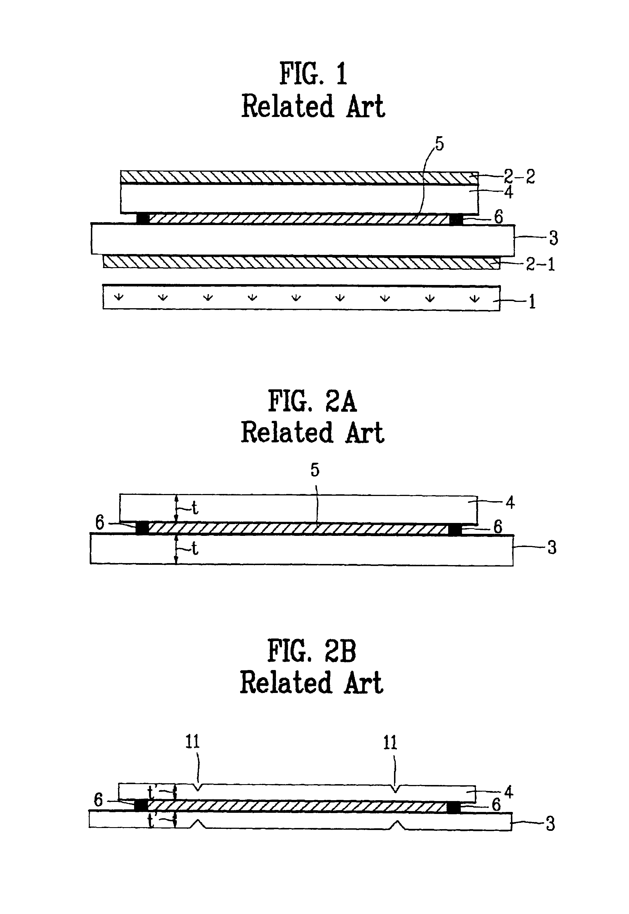
a technology of liquid crystal display and display device, which is applied in the field of can solve the problems of limiting the reduction of weight and size to the main elements of the liquid crystal display device, the thickness of the glass substrate is limited, and the glass substrate is broken during the processing or cracks are generated, so as to prevent the formation of the glass substrate

Inactive Publication Date: 2005-08-16
LG DISPLAY CO LTD
View PDF20 Cites 11 Cited by
  • Summary
  • Abstract
  • Description
  • Claims
  • Application Information

AI Technical Summary

Benefits of technology

[0024]An advantage of the present invention is to provide an LCD device and a method for manufacturing the same, in which a glass organic film such as benzocyclobutene (BCB) and photo-acrylate is deposited on a surface of a glass substrate damaged by etching and polishing processes, so as to repair the damaged surface of the glass substrate.
[0025]Additional advantages, and features of the invention will be set forth in part in the description which follows and in part will become apparent to those having ordinary skill in the art upon examination of the following or may be learned from practice of the invention. The objectives and other advantages of the invention may be realized and attained by the structure particularly pointed out in the written description and claims hereof as well as the appended drawings.
[0026]To achieve these and other advantages and in accordance with the purpose of the invention, as embodied and broadly described herein, an LCD device according to the present invention includes first and second substrates assembled together with some spaces therebetween, each having an etched outer surface; and a passivation film on an outer surface of the first and second substrates.
[0027]In another aspect of the present invention, a method for manufacturing an LCD device includes the steps of preparing first and second substrates; assembling the first and second substrates together, etching surfaces of the assembled first and second substrates, and forming a passivation film on the surfaces of the first and second substrates.
[0028]Herein, the passivation film includes an organic film. The organic film is formed by a spin-coating process. The organic film includes BCB or photo-acrylate. Also, the organic film is formed of a material in which a refractive index difference with the glass substrate is within about 10%.
[0029]In one embodiment of the present invention, the passivation film is formed on the glass substrate. Therefore, it is possible to prevent the glass substrate from being formed at an uneven thickness, which is generated by a scratch of the glass substrate when the glass substrate is unevenly etched.

Problems solved by technology

However, LCD structure and current technology limit the decrease of weight and size to the main elements of the LCD.
However, if the thickness decreases below a specific value, the glass substrate is broken during its processing or cracks are generated.
Therefore, there is a limitation in decreasing the thickness of the glass substrate.
This method, however, has disadvantages in that the glass substrate is disproportionally etched due to the incompleteness of the glass substrate itself, or foreign particles generated during the etching process stick to the etched surface of the glass substrate and thus the surface of the glass substrate becomes irregular.
This results in the occurrence of dot or spot defects on a screen during driving the LCD device.

Method used


Image

  • Liquid crystal display device and method for manufacturing the same
  • Liquid crystal display device and method for manufacturing the same
  • Liquid crystal display device and method for manufacturing the same

Examples


Embodiment Construction

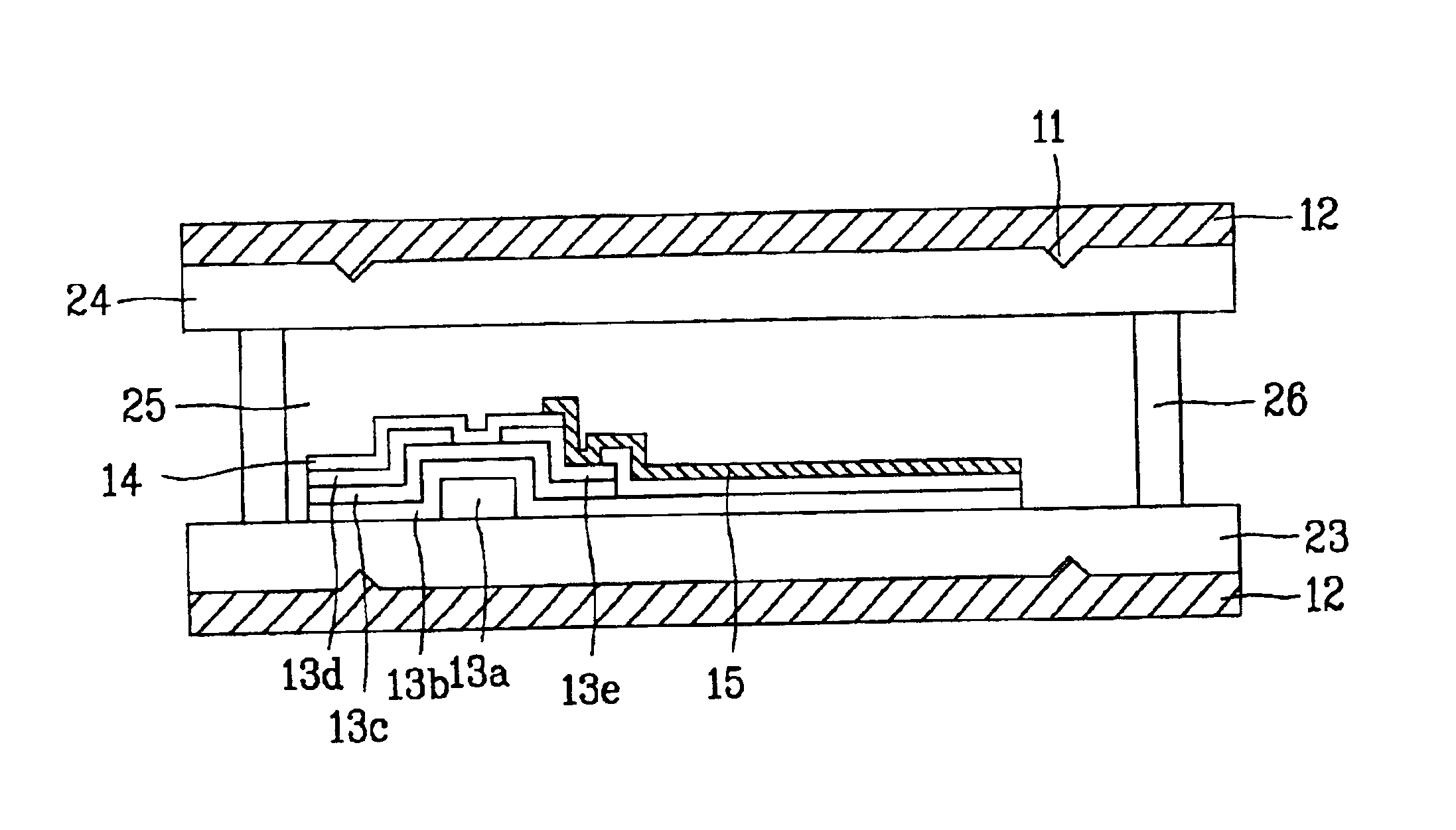
[0037]Reference will now be made in detail to an embodiment of the present invention, examples of which are illustrated in the accompanying drawings.

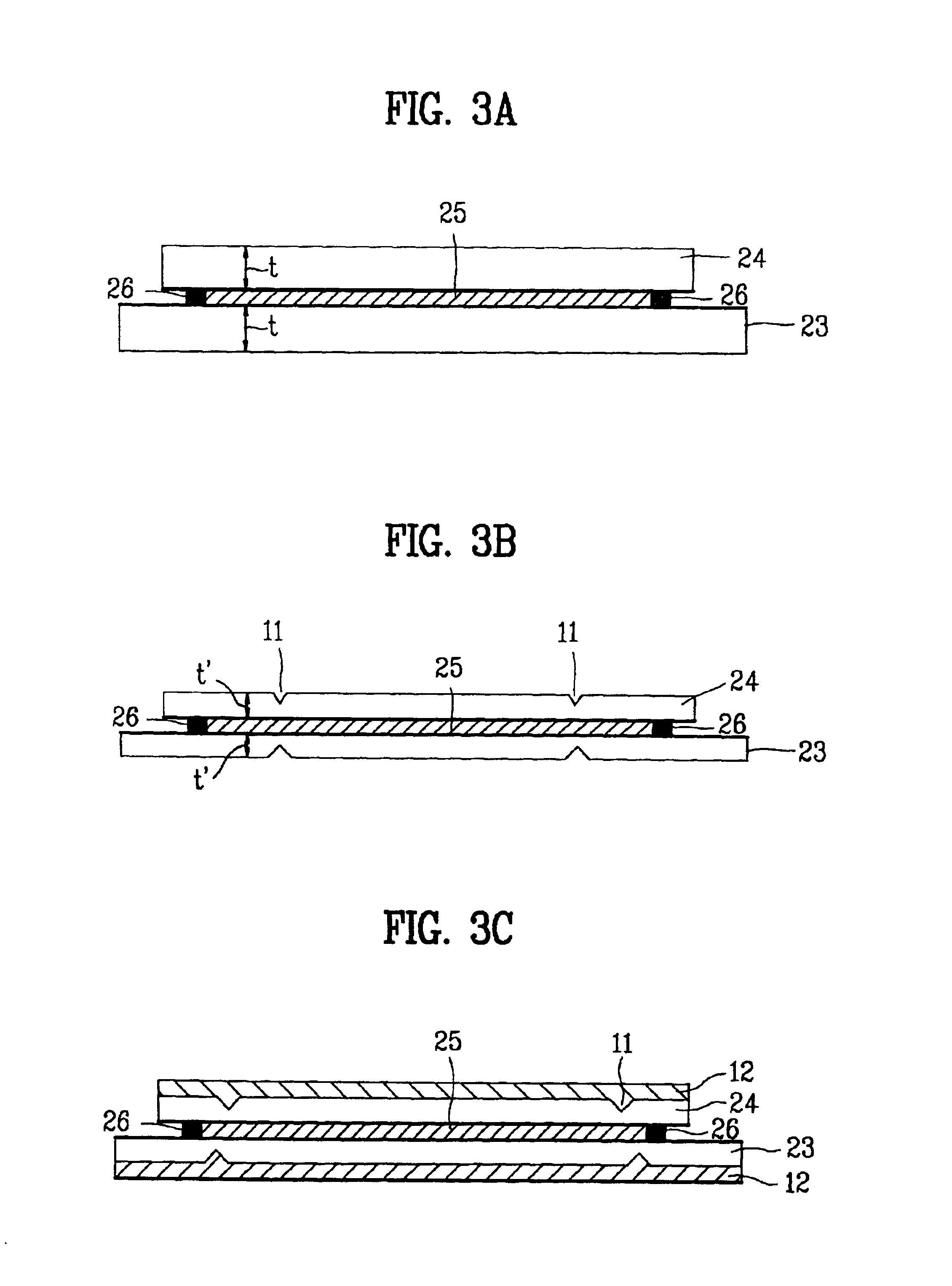
[0038]An LCD device and a method for manufacturing the same will be described with reference to FIG. 3A to FIG. 3C. First, as shown in FIG. 3A, a plurality of gate lines and data lines (not shown) are formed on a first glass substrate 23 at a thickness of “t” to define pixel regions of a matrix arrangement (not shown). Also, the gate lines are formed to cross the data lines. Then, a thin film transistor and a pixel electrode are formed in the respective pixel regions (not shown).

[0039]A black matrix layer (light-shielding layer), a color filter layer and a common electrode are formed on a second glass substrate 24 at a thickness of “t” (not shown).

[0040]Such first and second glass substrates are assembled together by a sealing pattern 26 to form some space between the substrates. As shown in FIG. 3A, a liquid crystal 25 is injected into...


PUM

PropertyMeasurementUnit
thicknessaaaaaaaaaa
thicknessaaaaaaaaaa
refractive indexaaaaaaaaaa

Abstract

A liquid crystal display device is disclosed, which can remove a defect generated from polishing and etching of a glass substrate. The LCD device includes first and second substrates assembled together with some spaces therebetween, each having an etched outer surface, and a passivation film outside the first and second substrates. In the LCD device, the passivation film such as BCB or photo-acrylate is formed on a surface of a glass substrate damaged by etching and polishing processes, so as to repair the damaged surface of the glass substrate.

Description

[0001]This application claims the benefit of Korean Patent Application No. P2000-85558, filed on Dec. 29, 2000, the entirety of which is hereby incorporated by reference for all purposes as if fully set forth herein.BACKGROUND OF THE INVENTION[0002]1. Field of the Invention[0003]The present invention relates to a liquid crystal display (LCD) device, and more particularly, to an LCD device and a method for manufacturing the same that can remove a defect generated from polishing and etching of a glass substrate.[0004]2. Background of the Related Art[0005]Recently, research of flat panel displays such as liquid crystal displays (LCD), plasma display panels (PDP), electroluminescent displays (ELD), vacuum fluorescent displays (VFD), etc., is being performed, and these displays are being used in various apparatuses.[0006]Among these displays, LCDs are most widely used in that they have good picture quality and low power consumption characteristics. They are being used as the display in p...

Claims


Application Information

Patent Timeline
Patent Type & Authority Patents(United States)
IPC IPC(8): G02F1/13G02F1/1333G02F1/1335G02F1/133
CPCG02F1/1333G02F1/133502G02F2001/133302G02F2201/50G02F1/133302G02F1/133
Inventor MOON, HONG MAN
Owner LG DISPLAY CO LTD
Why Eureka
Try Eureka