Sector synchronized test method and circuit for memory

a test method and memory technology, applied in the field of test methods and test circuits for memory, can solve the problems of increasing memory capacity, longer time for program and erase operations, etc., and achieve the effect of reducing the whole test time of the wafer or ic, and shortening the time required for performing program and erase operations on the memory

Inactive Publication Date: 2005-08-16
MACRONIX INT CO LTD
View PDF6 Cites 7 Cited by
  • Summary
  • Abstract
  • Description
  • Claims
  • Application Information

AI Technical Summary

Benefits of technology

[0009]The invention provides a sector synchronized test method and circuit. By providing more test channels for the circuit, program and erase operation is performed on more dies or IC's at a time. Therefore, the time required for performing program and erase operations on the memory is shortened, and the whole test time of the wafer or IC is decreased.

Problems solved by technology

For example, the capacity of a memory becomes increasingly large.
Thus, the more the capacity of the memory is, the longer time the program and erase operations take.

Method used


Image

  • Sector synchronized test method and circuit for memory
  • Sector synchronized test method and circuit for memory
  • Sector synchronized test method and circuit for memory

Examples


Embodiment Construction

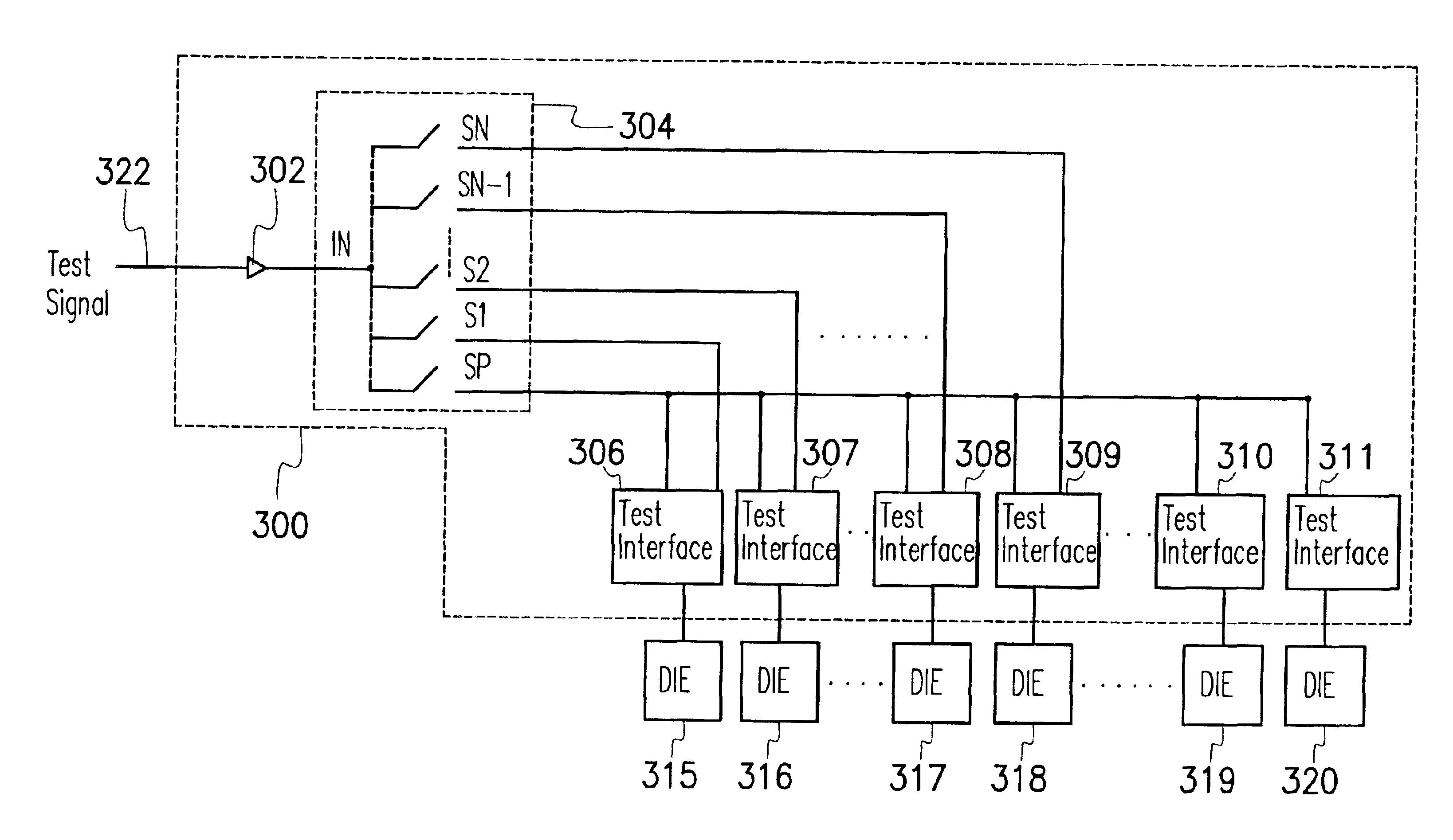
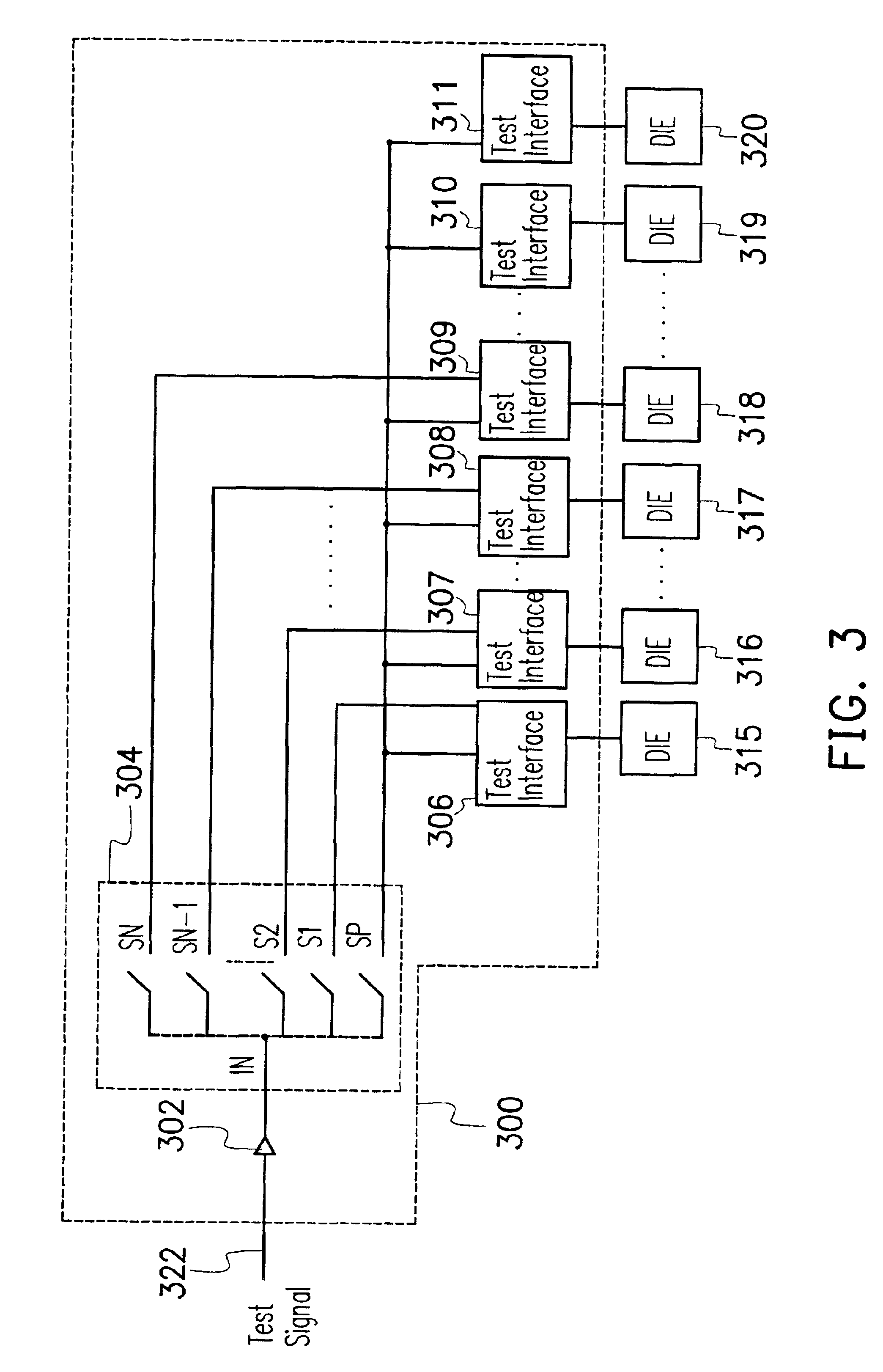
[0019]FIG. 3 shows the sector synchronized test circuit for a memory provided by the invention. While performing a DC test on a memory die 315 to 320, the direct test power source or signal bus 322 (data transfer in both directions) is sent from the read-write device 302 to the input terminal IN of the selected switch 304. According to the channel connected by the selected switch 304 on one of the memory die 315 to 320, the DC test is performed on one of the memory dies. For example, when the output terminal S1 is connected with the selected switch 304, the direct test power source or signal bus and test interface 306 will perform a DC test on memory die 315. Similarly, when the output terminals S2, . . . , SN-1, SN of the selected switch 304 are connected, the direct test power source or signal bus and test interface 307, . . . , 308, 309 will perform a DC test on memory die 316, . . . , memory die 317, and memory die 318. When the memory dies, which are waiting to be tested are in...


PUM


Abstract

A sector synchronized test method and circuit for a memory, applicable for testing several electrically programmable or electrically erasable memory dies. The section synchronize test circuit has a read-write device, a selected switch, and a plurality of test interfaces. While programming or erasing the memory dies simultaneously, the selected switch connects the parallel output terminal, so that the memory dies are connected in parallel. Meanwhile, the read-write device receives a test signal to perform the program or erase operation on the memory dies according to the test signal.

Description

CROSS-REFERENCE TO RELATED APPLICATION[0001]This application claims the priority benefit of Taiwan application serial no. 90121413, filed Aug. 30, 2001.BACKGROUND OF THE INVENTION[0002]1. Field of the Invention[0003]The invention relates in general to a test method and a test circuit for a memory, and more particularly, to a sector synchronized test method and circuit for a memory.[0004]2. Description of the Related Art[0005]FIG. 1 shows a schematic drawing of a wafer. As the semiconductor technique is more and more advanced, each die 102 of a wafer 100 comprises more and more transistor circuits. For example, the capacity of a memory becomes increasingly large. For a memory die such as erasable programmable or electrically erasable programmable memory die, the power consumption has to be reduced.[0006]With regard to the erasable programmable or electrically erasable programmable memory, the yield test of the wafer has to be performed after completing the fabrication of integrated c...

Claims


Application Information

Patent Timeline
Patent Type & Authority Patents(United States)
IPC IPC(8): G11C29/04G11C29/48G11C29/26G11C29/52
CPCG11C29/26G11C29/48G11C29/52G11C2029/2602
Inventor LAY, SHYAN-JER
Owner MACRONIX INT CO LTD
Why Eureka
Try Eureka