Electronic component testing socket and electronic component testing apparatus using the same

a technology for electronic components and testing sockets, which is applied in the direction of testing/measurement of semiconductor/solid-state devices, coupling device connections, instruments, etc., can solve the problems of difficult air circulation in the chamber, inability to maintain the ic socket and the ic device to be tested, and contact credibility, etc., to reduce the effect of thermal stress and suppress the reduction of thermal stress

Inactive Publication Date: 2005-08-23
ADVANTEST CORP
View PDF8 Cites 20 Cited by
  • Summary
  • Abstract
  • Description
  • Claims
  • Application Information

AI Technical Summary

Benefits of technology

[0016]An object of the present invention is to provide an electronic component testing socket capable of efficiently controlling the temperature of an electronic component testing socket, such as an IC socket, without mixing any noise in a test signal to be applied to the electronic component, such as an IC device, and a respond signal to be read from the electronic component, such as an IC device, by using a temperature controlled gas, an electronic component testing socket base, an electronic component testing unit, an electronic component testing apparatus, and a method of controlling the temperature of the electronic component testing socket. Note that in the present specification, the words “to control the temperature of the electronic component testing socket” are meant to include both maintaining and changing the temperature of the electronic component testing socket to be a desired temperature.
[0077]Furthermore, in the method of controlling the temperature of the electronic component testing socket of the present invention, since it is possible to successively or intermittently flow a thermoregulated gas to the space formed inside the electronic component testing socket, it makes the electronic component testing socket hard to be affected by a temperature change due to a heat transfer via the contact portion with the outside (for example, an outside air), and thereby, the temperature of the electronic component testing socket can be accurately controlled.

Problems solved by technology

In the case of considering a thermal stress being eased on the IC device to be tested to set the temperature in the chamber to make up for the loss in advance, however, although a desired thermal stress can be applied to the IC device under testing, an excessive thermal stress is given to an IC device standing by in the chamber, so that the contact credibility of the IC device to be tested and the IC socket cannot be maintained.
Also, when circulating an air in the chamber to the lower side of the socket board, there are much physical obstacles, such as, many cables and board under the socket board, so it is difficult to circulate the air in the chamber thereto and it becomes costly when trying to forcibly circulate the air.
Also, since the space under the mother board became a low temperature, there arises dew condensation on the lower side of the mother board when circulating the air in the chamber between the socket board and the mother board.
To prevent the condensation, the mother board has to be sealed or a dry air has to be injected to the lower side of the mother board, which ends up in the complicated configuration.
Further, when providing a heat source or a cool source using electricity to the socket guide mounted on the IC socket, in the IC device test, the performance and function of the IC device to be tested are tested by applying a test signal to the IC device and reading a response signal from the IC device, and if a noise generated from an effect of electricity used by the heat source or cool source mixes in the test signal to be tested to the IC device and the respond signal read from the IC device, accuracy of the test declines or the test may not be able to be continued under some circumstances.

Method used


Image

  • Electronic component testing socket and electronic component testing apparatus using the same
  • Electronic component testing socket and electronic component testing apparatus using the same
  • Electronic component testing socket and electronic component testing apparatus using the same

Examples


first embodiment

[0110

[0111]An embodiment of a chamberless type (a heat plate type) will be explained as a first embodiment of the present invention based on the drawings.

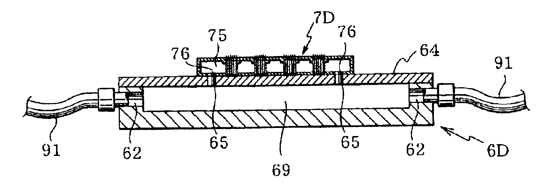
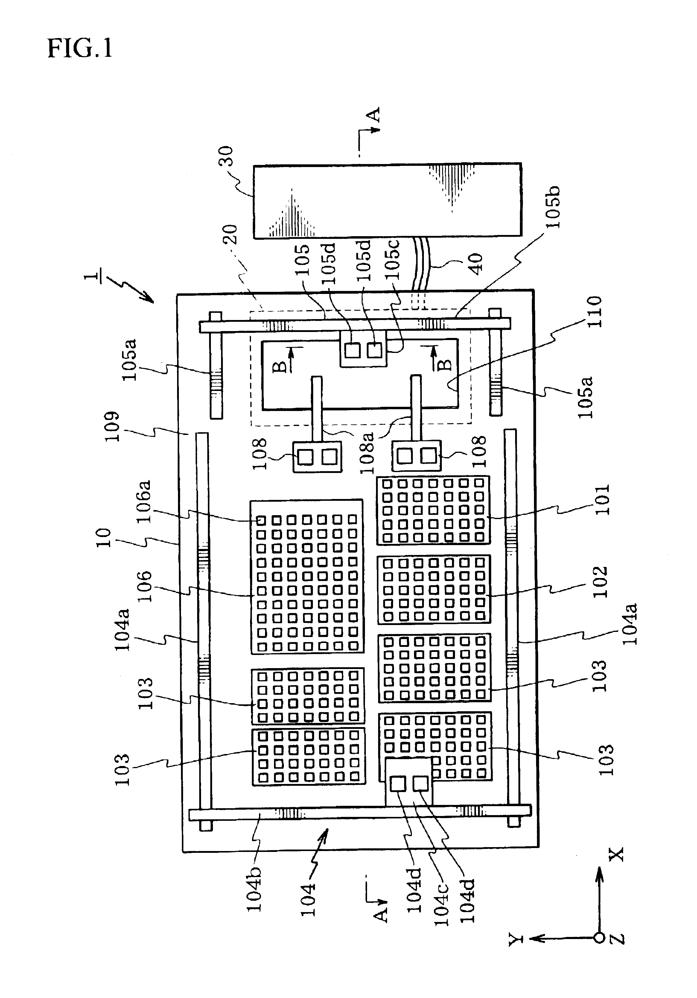
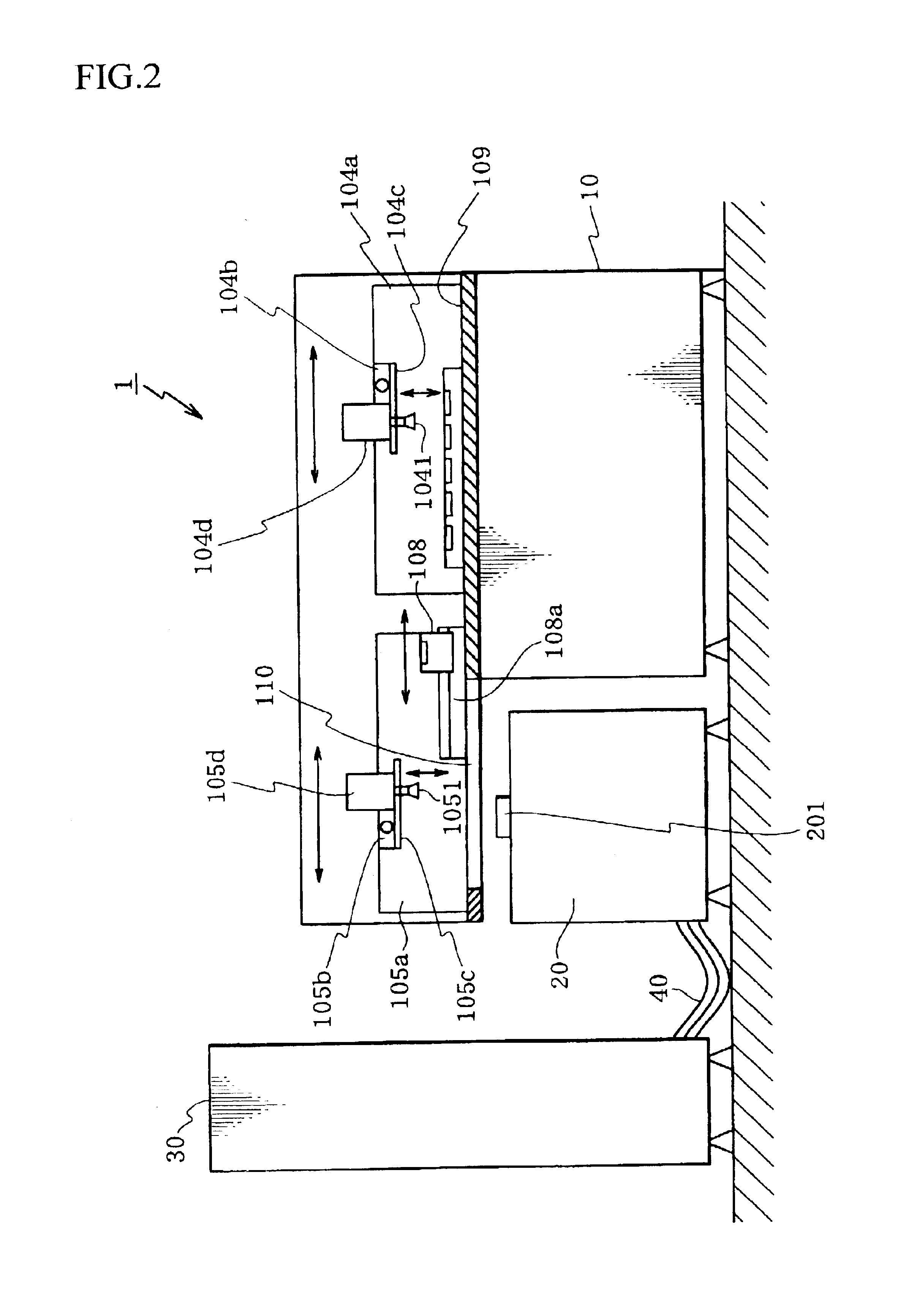
[0112]FIG. 1 is a plan view of an embodiment of an electronic component testing apparatus wherein an electronic component testing unit according to the present invention is applied, FIG.2 is a cross sectional view along the line A—A in FIG. 1, FIG. 3 is a cross sectional view (a cross sectional view along the line B—B in FIG. 1) of a contact section of the test head in detail, FIG. 4(a) is a view from above of an embodiment of an electronic component testing unit according to the present invention, FIG. 4(b) is a cross sectional view along the line A—A in FIG. 4(a), FIG. 4(c) is a cross sectional view along the line B—B in FIG. 4(a), FIG. 5(a) is a view from above of an embodiment of an electronic component testing socket according to the present invention, FIG. 5(b) is a cross sectional view along the line A—A in FIG. 5(a), FIG. 5...

second embodiment

[0187

[0188]An embodiment of a chamber type will be explained as a second embodiment of the present invention based on the drawings.

[0189]FIG. 13 is an overall view from the side of an IC testing apparatus according to an embodiment of an electronic component testing apparatus of the present invention, FIG. 14 is a perspective view of a handler in the IC testing apparatus, FIG. 15 is a flow chart of movement of a tray showing a method of handling an IC to be tested, FIG. 16 is a perspective view of the structure of an IC stocker in the IC testing apparatus, FIG. 17 is a perspective view of a customer tray used in the IC testing apparatus, FIG. 18 is a cross sectional view of important parts in a test chamber in the IC testing apparatus, FIG. 19 is a partially disassembled perspective view of a test tray used in the IC testing apparatus, FIG. 20 is a disassembled perspective view of the configuration around a socket in a test head of the IC testing apparatus, FIG. 21 is a disassembled...


PUM


Abstract

To control the temperature of an electronic component testing socket without mixing any noise into a test signal to be applied to an electronic component and a respond signal to be read from the electronic component when conducting a test on the electronic component, a first space 67 in the electronic component testing socket base 6 and a socket body inside space 75 in the electronic component testing socket 7 are connected via a gas outlet 65 and a gas inlet 76, and a second space 68 in the electronic component testing socket base 6 and a socket body inside space 75 in the electronic component testing socket 7 are connected via a gas inlet 66 and a gas outlet 77.

Description

[0001]This application is a con. of PCT / JP01 / 10729 filed Dec. 07, 2001.BACKGROUND OF THE INVENTION[0002]1. Field of the Invention[0003]The present invention relates to an electronic component testing socket used for loading an electronic component to be tested in an electronic component testing apparatus for testing performance and functions of an electronic component, such as in IC device and an electronic component testing socket base used for mounting the electronic component testing socket. Also, the present invention relates to an electronic component testing unit wherein the electronic component testing socket is mounted on the electronic component testing socket base and an electronic component testing apparatus wherein the electronic component testing socket or an electronic component testing unit is mounted.[0004]2. Description of the Related Art[0005]In a production process of an electronic component, such as an IC device, an electronic component testing apparatus for test...

Claims


Application Information

Patent Timeline
Patent Type & Authority Patents(United States)
IPC IPC(8): G01R31/01G01R31/28G01R1/04G01R1/02G01R31/26G01R1/06G01R1/073H01R33/76
CPCG01R31/01G01R31/2863G01R1/0458G01R1/0408H01L22/00
Inventor ISHIKAWA, TAKAJINAKAMURA, HIROTO
Owner ADVANTEST CORP
Why Eureka
Try Eureka