VCSEL packaging

a technology of vcsel and packaging, applied in the direction of sustainable manufacturing/processing, final product manufacturing, soldering apparatus, etc., can solve the problems of difficult to maintain a large size chip flat, different parts of the vcsel chip may warp differently, and require different pressure or force, so as to improve thermal and electrical performance.

Active Publication Date: 2015-05-26
PRINCETON OPTRONICS
View PDF54 Cites 20 Cited by
  • Summary
  • Abstract
  • Description
  • Claims
  • Application Information

AI Technical Summary

Benefits of technology

[0019]The soldering processes for the VCSELs and arrays in the invention include fluxless vacuum soldering processes for significantly improved thermal and electrical performance. The mechanical configuration for this invention of the VCSEL arrays on submounts and contact bonding to the printed circuit board enable bonding of a temperature control or cooling device to the submount or printed circuit board resulting in efficient cooling or temperature control of the VCSEL array.

Problems solved by technology

While several of the commonly known methods used for packaging electronic components including integrated circuits (ICs) may be adapted for packaging VCSELs and VCSEL arrays or VCSEL array chips with or without additional electronic components, applying the same methods to large size VCSEL arrays ranging from several millimeters to a centimeter in linear dimensions, is still challenging.
One particular problem arises from the fact that it is difficult to maintain a large size chip flat during the packaging process.
This problem is particularly a challenge when the VCSEL chip is made thin or ultra-thin for better heat dissipation, and tends to warp.
Furthermore, different parts of the VCSEL chip may warp differently and require different pressure or force while packaging.

Method used


Image

  • VCSEL packaging
  • VCSEL packaging
  • VCSEL packaging

Examples


Embodiment Construction

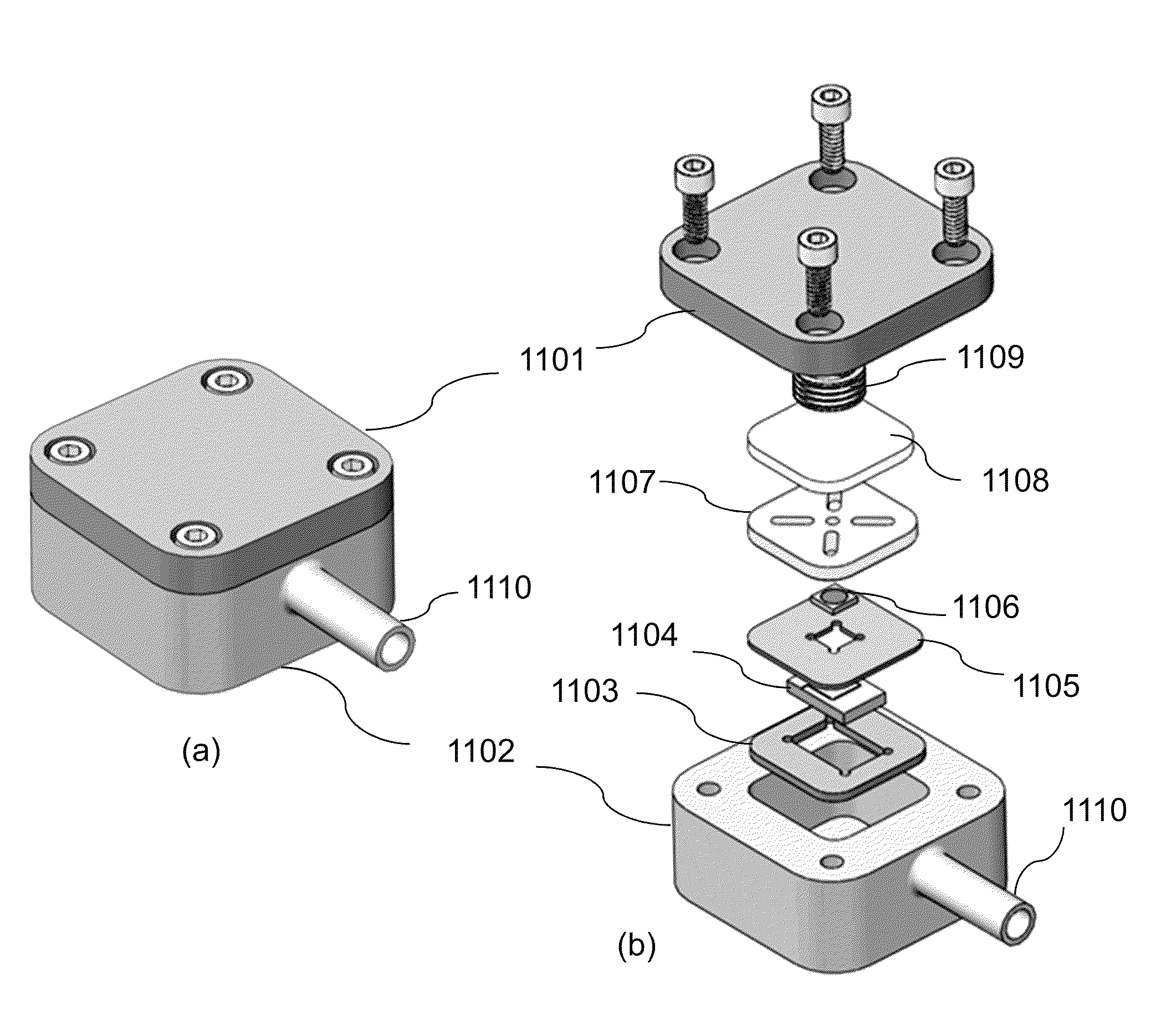
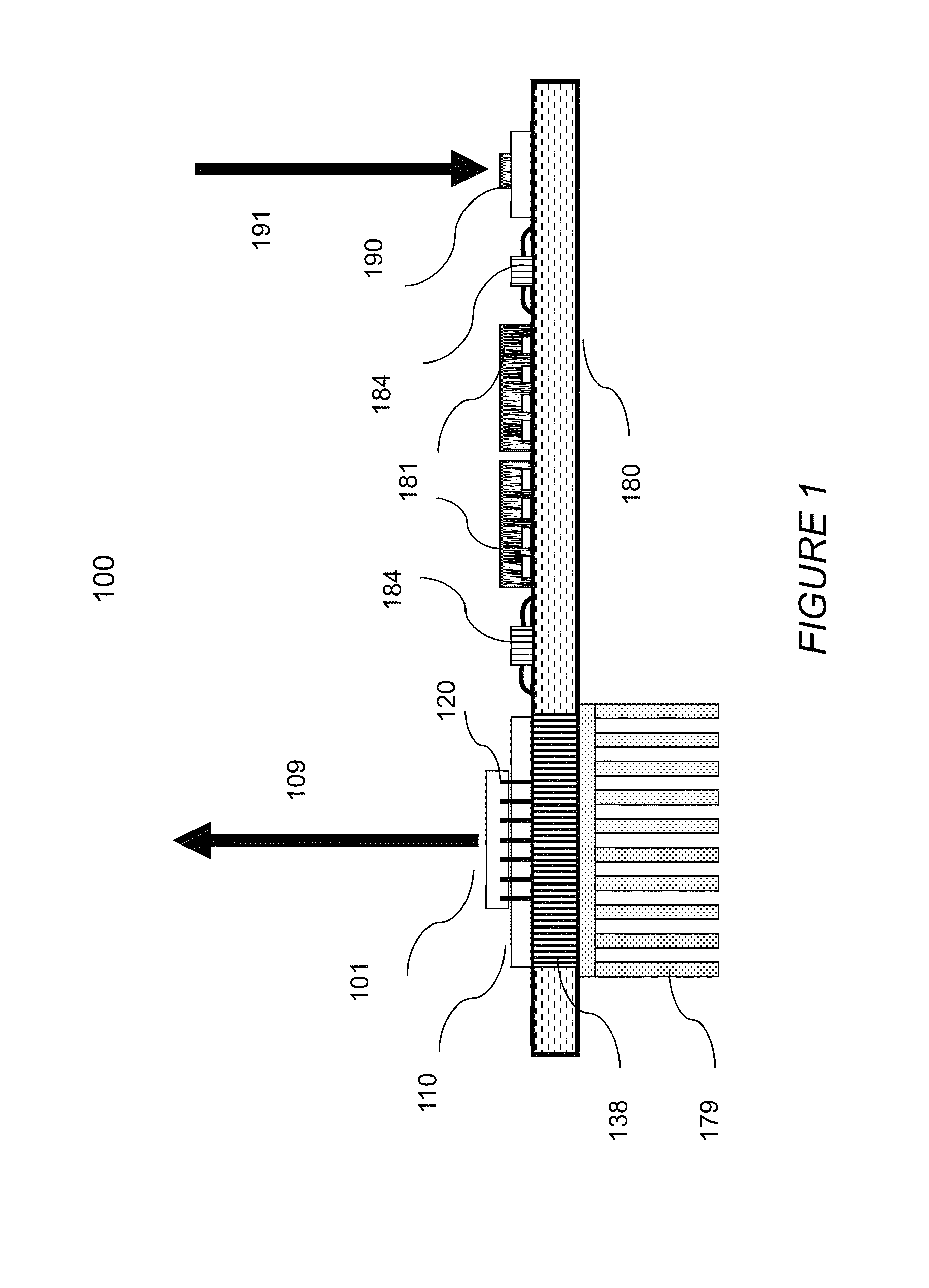
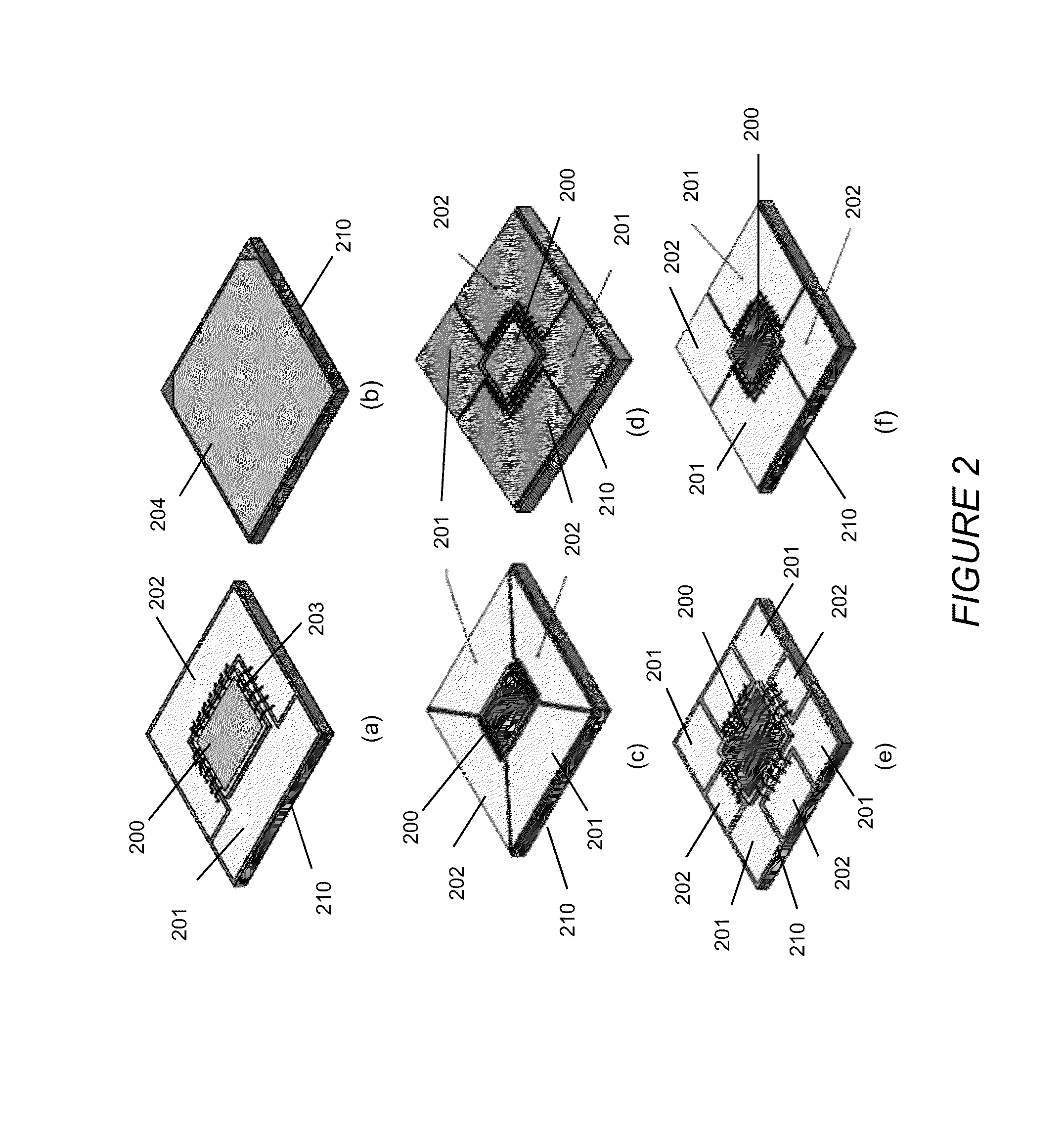
[0033]Different aspects of packaging VCSELs for incorporating them in functional modules with or without additional electronic components will be described using illustrations and explanations. One important aspect of this invention is to incorporate means and methods for integrating optical modules with electronic components in a packaging process to ensure that the VCSEL devices (individual and / or arrays) and in particular, VCSEL devices having a large area array are optically flat. The method is particularly suited for applications where it is necessary to ensure that all VCSELs in an array emit not only in the same direction but also at a substantially same angle in reference with a normal to the emission surface and will be elaborated later.

[0034]Each illustration includes only a few aspects to explain the basic concepts of the invention. However, within a broad framework of the invention different aspects from different illustrations may be combined or practiced separately to ...


PUM

PropertyMeasurementUnit
pressureaaaaaaaaaa
angle of reflectionaaaaaaaaaa
fix angleaaaaaaaaaa

Abstract

A process to bond VCSEL arrays to submounts and printed circuit boards is provided. The process is particularly suited to large area thin and ultra-thin VCSEL arrays susceptible to bending and warping. The process integrates a flatness measurement step and applying appropriate combination of pressure prior to bonding the VCSEL array to the submount or a printed circuit using a vacuum flux-less bonding process. The process is very promising in making very good quality bonding between the VCSEL array and a submount or a printed circuit board. The process is applied to construct optical modules with improved flatness that may be integrated with other electronic components in constructing optoelectronic systems.

Description

CROSS REFERENCE TO RELATED APPLICATION[0001]This application claims priority benefit from the U.S. Provisional Patent Application No. 61 / 876,302 filed on Sep. 11, 2013, the contents of which is being incorporated by reference in their entirety.BACKGROUND OF THE INVENTION[0002]1. Field of Invention[0003]The present invention relates to packaging of VCSELs and in particular to large size arrays of VCSELs on submounts and / or on printed circuit boards with other electronic components including current drivers, optical and electronic sensor systems, data storage and data processors, to incorporate multiple functionalities to achieve high optical power illumination, irradiation 2 and 3-dimensional imaging and 3-dimensional (3-D) printing systems.[0004]2. Related Background Art[0005]In the last few years lasers, and more especially VCSELs and VCSEL arrays, have found applications as sources for optical systems for high power illumination for general illumination, optical pumps for lasers a...

Claims


Application Information

Patent Timeline
Patent Type & Authority Patents(United States)
IPC IPC(8): B23K31/02B23K1/00H01S5/00H01S5/022
CPCH01S5/02272H01S5/0042B23K1/0016H01S5/423H05K1/0206H05K3/3436H05K3/3494H05K2201/10121H05K2201/10727H05K2203/085B23K1/012H01L2224/16225H01L2224/48091H01L2224/49175B23K2101/42Y02P70/50H01S5/0237H01S5/02345H01L2924/00014
Inventor WANG, QINGSEURIN, JEAN-FRANCOISGHOSH, CHUNI LALWATKINS, LAURENCE
Owner PRINCETON OPTRONICS
Why Eureka
Try Eureka