Eureka AIR delivers breakthrough ideas for toughest innovation challenges, trusted by R&D personnel around the world.

Method of producing thermistor chips

Inactive Publication Date: 2005-08-30
MURATA MFG CO LTD
View PDF18 Cites 0 Cited by
  • Summary
  • Abstract
  • Description
  • Claims
  • Application Information

AI Technical Summary

Benefits of technology

[0006]It is therefore an object of this invention in view of the problems of prior art technology outlined above to provide a method of producing thermistor chips by a simplified process of dipping a thermistor body in a solvent in order to partially melt away its externally exposed surfaces and to thereby increase the resistance between the outer electrodes such that thermistor chips can be produced with resistance values which are within a reduced range around a specified target value.

Problems solved by technology

If prior art technology is used for this process, however, the thermistor chip is heated up by the energy of the laser and the thermistor body generates small cracks, causing variations in the resistance values of thermistor chips after the trimming process.
Another problem with this prior art technology is that a laser beam must be made incident individually on each of many thermistor chips to be produced for trimming.
This means that the process is cumbersome to carry out and contributes to an increase in the production cost.

Method used


Image

  • Method of producing thermistor chips
  • Method of producing thermistor chips
  • Method of producing thermistor chips

Examples


Embodiment Construction

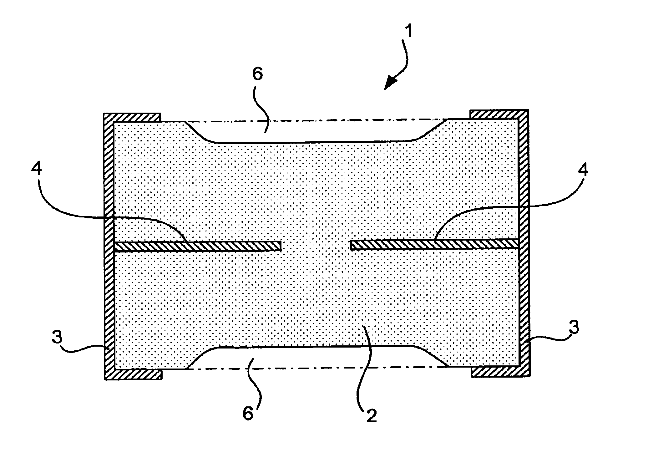
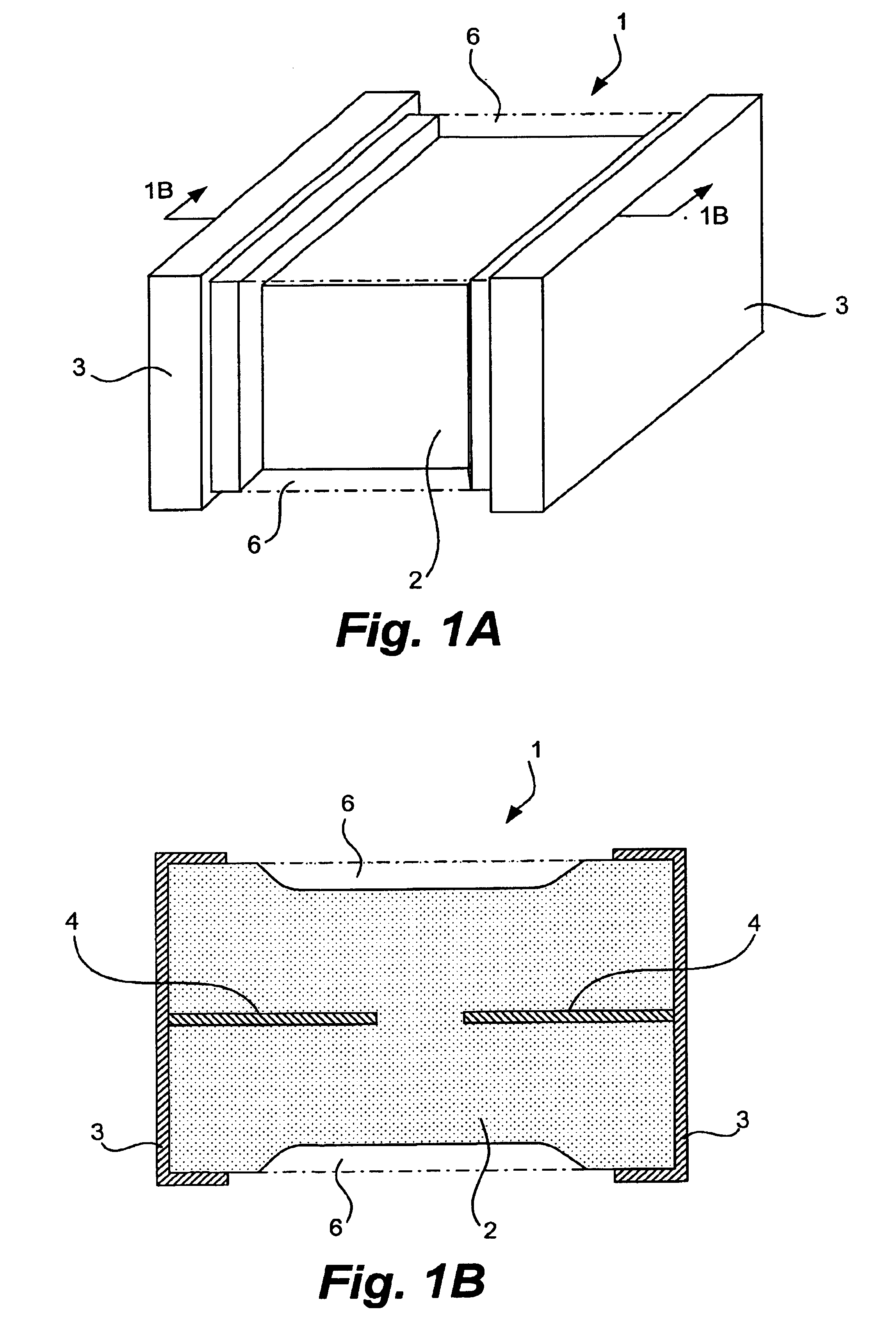
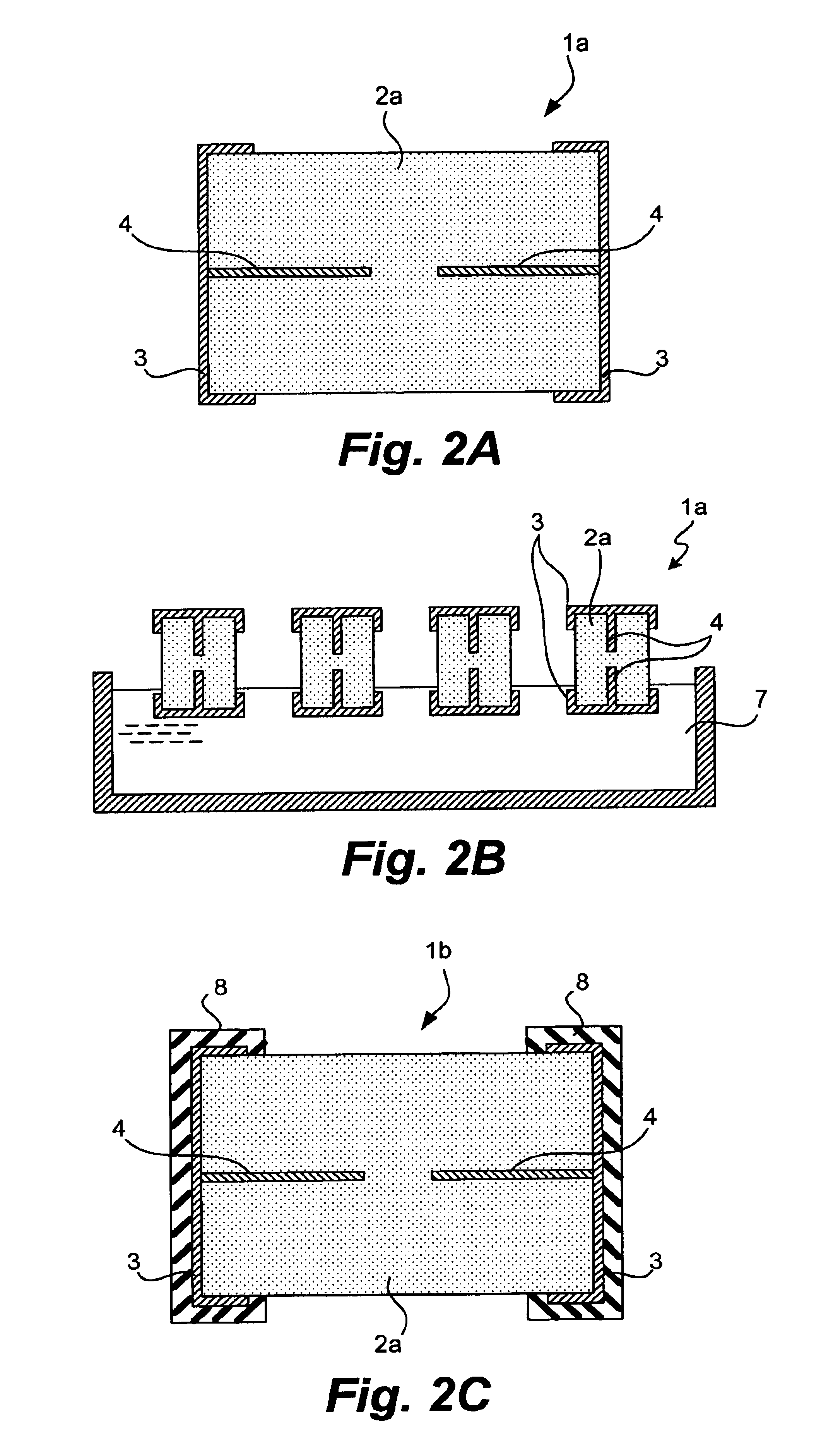
[0019]The invention is described next by way of an example. FIGS. 1A and 1B show a thermistor chip 1 embodying this invention, comprising a thermistor body 2, outer electrodes 3 and inner electrodes 4 and being characterized wherein that the thermistor body 2 has portions which have been melted away and indented (referred to as the “melted portions 6”). The thermistor body 2 comprises a semiconducting ceramic material having oxides of a plurality of transition metals such as Mn, Ni, Co, Fe, Cu and Al. Portions of the thermistor body surface except where the outer electrodes 3 are formed on mutually opposite end parts of the thermistor body 2 are melted away by a solvent 10 (shown in FIG. 3A and to be explained below) to form the indented melted portions 6. The inner electrodes 4 are formed inside the thermistor body 2 such that their inner end parts are opposite to each other while the outer end part of each is electrically connected to a corresponding one of the outer electrodes 3....


PUM

PropertyMeasurementUnit
Lengthaaaaaaaaaa
Concentrationaaaaaaaaaa
Electrical resistanceaaaaaaaaaa

Abstract

Thermistor chips are produced by preparing thermistor bodies each having outer electrodes formed on its end parts and dipping them in a solvent so as to melt away exposed surface portions of the thermistor body. In order to efficiently adjust their resistance values so as to produce thermistor chips with resistance values having only small variations from a target value, the resistance value between the outer electrodes are measured for each and they are divided into ranks according to the measured resistance values, and the dipping process is carried out differently for different ranks such that different amounts of the thermistor body material will be melted away.

Description

[0001]This is a divisional of application Ser. No. 09 / 487,158 filed Jan. 19, 2000, now abandoned.BACKGROUND OF THE INVENTION[0002]This invention relates to methods of producing thermistor chips which may find use in temperature compensating circuits and temperature detecting elements.[0003]FIG. 8 shows an example of a prior art thermistor chip 41 of this type disclosed in Japanese Patent Publication Tokkai 7-74006, characterized as comprising a thermistor body 42, outer electrodes 43, inner electrodes 44 and a surface electrode 45. The thermistor body 42 comprises a semiconducting ceramic material having oxides of Mn, Ni and Co as its main component. The outer electrodes 43 are formed on mutually opposite end parts of the thermistor body 42. The inner electrodes 44 are formed inside the thermistor body 44 and each electrically connected to a corresponding one of the outer electrodes 43. The surface electrode 45 is formed on one of the surfaces of the thermistor body 42 and is separa...

Claims


Application Information

Patent Timeline
IPC IPC(8): H01C7/04H01C17/24H01C17/22H01C7/02
CPCH01C7/04H01C17/2416Y10T29/49085Y10T29/49099Y10T29/49082Y10T29/49083
Inventor FUJIMOTO, MITSUAKIFURUKAWA, NOBORUKAWASE, MASAHIKOKITO, NORIMITSU
Owner MURATA MFG CO LTD
Why Eureka
Eureka Blog
Learn More