Liquid crystal display having domain dividers

a liquid crystal display and domain divider technology, applied in the field of liquid crystal display, can solve the problems of not having a wide viewing angle of proposed structures and the viewing angle of vatn lcd may not be so wide, and achieve the effect of reducing disclination due to the disorder of liquid crystal molecules and wide viewing angl

Inactive Publication Date: 2005-08-30
SAMSUNG DISPLAY CO LTD
View PDF16 Cites 70 Cited by
  • Summary
  • Abstract
  • Description
  • Claims
  • Application Information

AI Technical Summary

Benefits of technology

[0022]The shape of the first and the second electrodes according to the present invention makes the liquid crystal layer therebetween to be divided into four regions having different average directi

Problems solved by technology

However, the viewing angle of the VATN LCD may not be so wide due to the difference in retardation values among viewing directions.

Method used


Image

  • Liquid crystal display having domain dividers
  • Liquid crystal display having domain dividers
  • Liquid crystal display having domain dividers

Examples


first embodiment

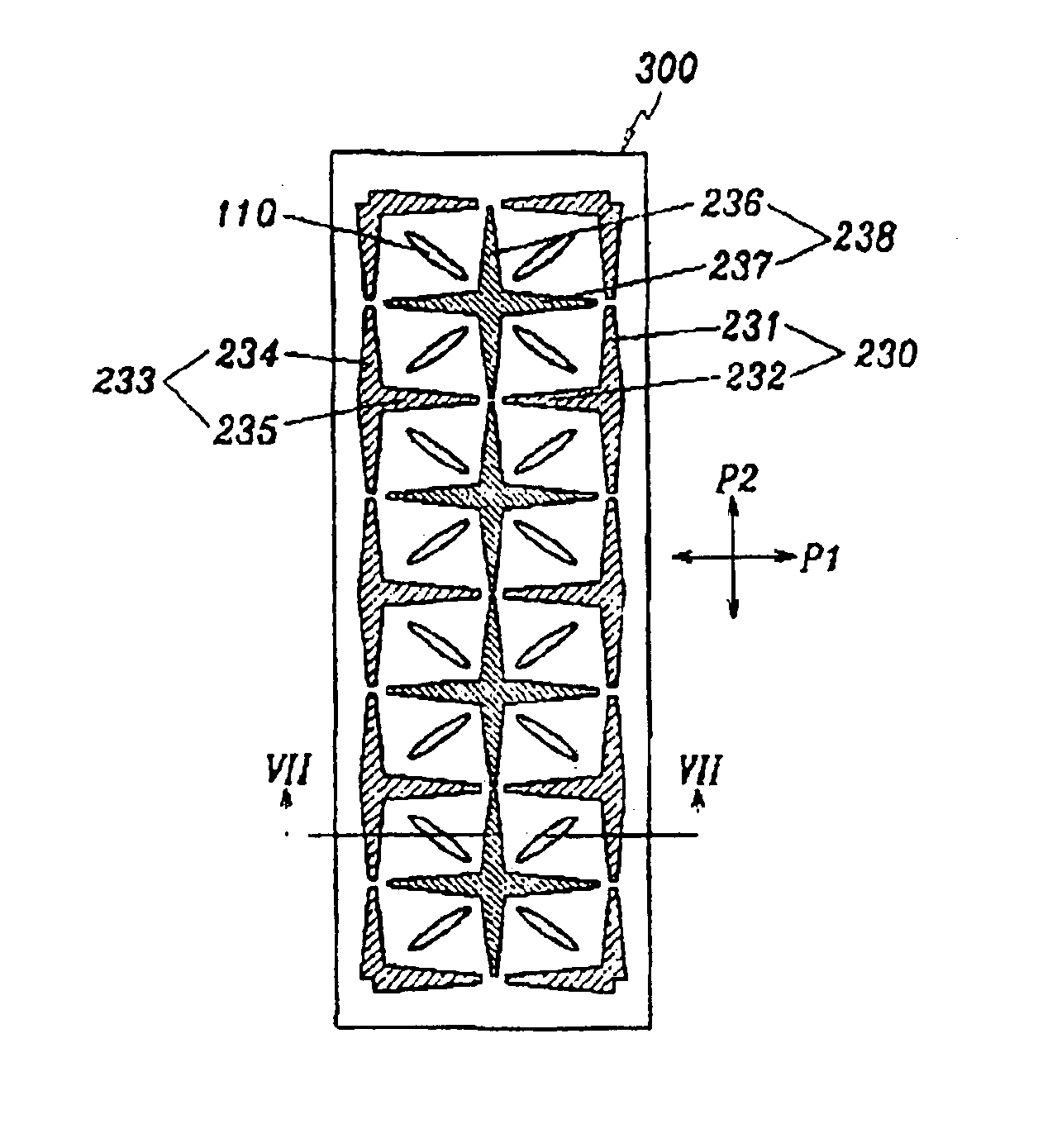
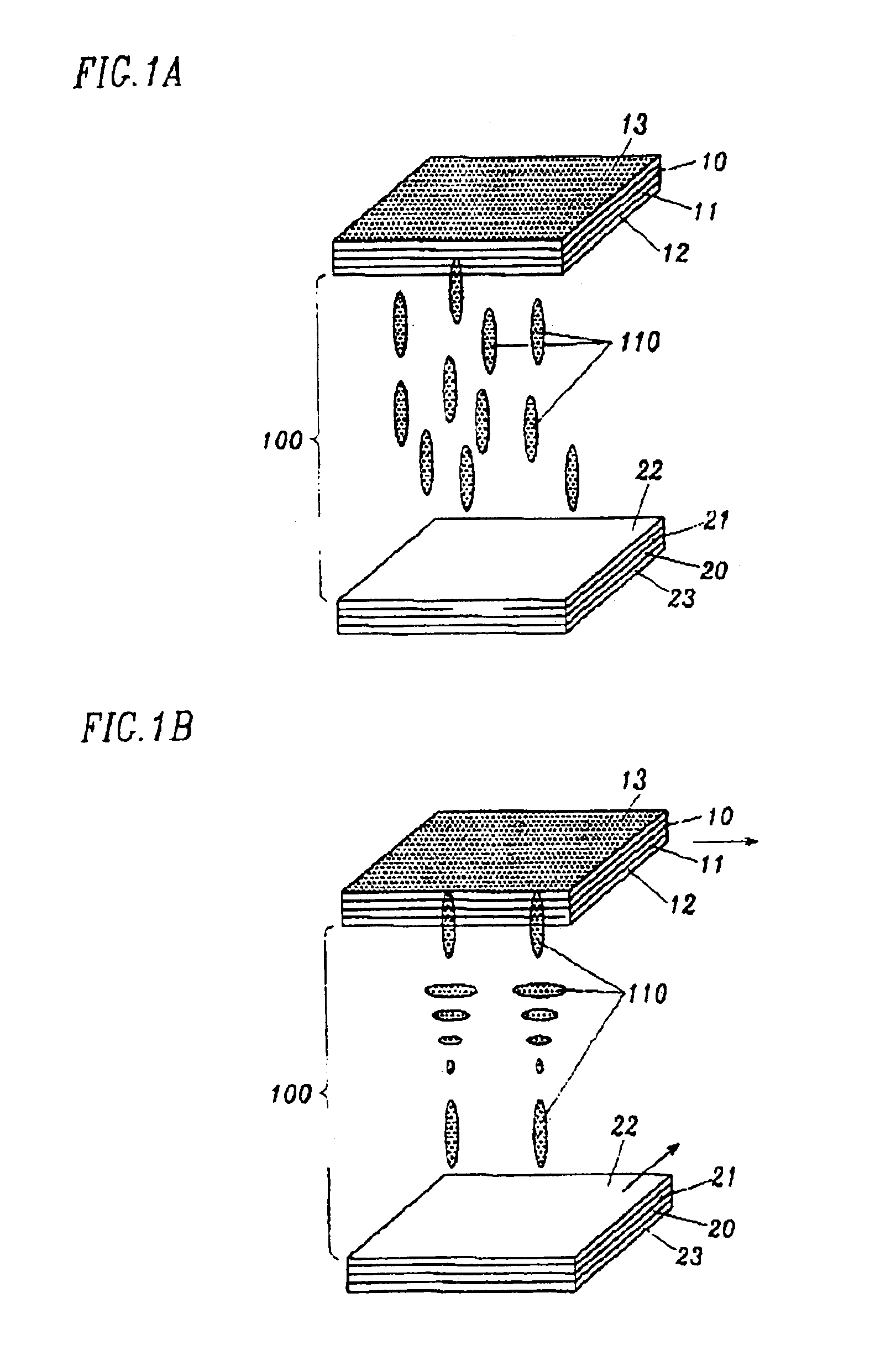
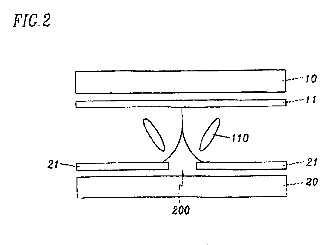
[0052]Now, considering these conditions, the present invention will be described with reference to FIGS. 3 and 4. Although an LCD has a plurality of pixels, FIGS. 3 and 4 show a single pixel region 300. In addition, only aperture patterns are illustrated in FIGS. 3 and 4, and other elements such as TFTs, wires, etc., are not illustrated.

[0053]As shown in FIGS. 3 and 4, a plurality of linear apertures 211, 212, 216 and 217 are formed in a rectangular pixel region 300. A plurality of first and second apertures 211 and 212 extending in transverse and longitudinal directions respectively are formed in an electrode 11 on an upper substrate 10, and a cross-shaped aperture 216 and 217 including first and second portions 216 and 217 extending in the transverse and longitudinal directions respectively are formed in an electrode 21 on a lower substrate 20.

[0054]The first and the second apertures 211 and 212 are separated from each other, arranged in the longitudinal direction, and form four l...

second embodiment

[0062]An aperture pattern according to the present invention shown in FIG. 5 is similar to the aperture pattern shown in FIG. 3 except for rectangular shape of the domains instead of square shape. That is, longitudinal apertures 221 and 226 are longer than transverse apertures 222 and 227. Accordingly, when viewed from the top, an angle made by the average axial directions in the adjacent domains is not exactly 90°, and an angle between the polarizing directions and the average axial directions is not exactly 45°. However, in this case, one of the transverse or longitudinal directions is preferred by the liquid crystal molecules because the long axes of the liquid crystal molecules makes a less angle with one of the two directions than with the other. Since the rearrangement of the liquid crystal molecules quickly occurred and becomes stable, the response time is relatively short than the LCD shown in FIG. 3.

[0063]A liquid crystal display exhibiting less response time is now describ...

third embodiment

[0064]FIG. 6 is a layout view of an aperture pattern of an LCD according to the present invention, and FIG. 5 is a sectional view of the LCD shown in FIG. 6 taken along the line VII-VII′.

[0065]As shown in FIGS. 6 and 7, an LCD according to the third embodiment of the present invention includes a lower TFT (thin film transistor) panel 20 and an upper color filter panel 10. Though it is not shown in the figures, a plurality of gate lines and data lines are formed on the inner surface of the TFT panel 20, and a pixel electrode 20 and a TFT (now shown) as a switching element are formed in a lower pixel region surrounded by the gate lines and data lines. On the inner surface of the color filter panel 10 opposite to the TFT panel 20, a black matrix pattern 14 which defines an upper pixel region corresponding to the lower pixel region in the TFT panel is formed, and a color filter 15 is formed therebetween. A passivation layer 16 covers the black matrix 14 and the color filter 15, and a co...


PUM


Abstract

A tetragonal ring shape aperture is formed in the common electrode on one substrate and a cross shape aperture is formed at the position corresponding to the center of the tetragonal ring shape aperture in the pixel electrode on the other substrate. A liquid crystal layer between two electrodes are divided to four domains where the directors of the liquid crystal layer have different angles when a voltage is applied to the electrodes. The directors in adjacent domains make a right angle. The tetragonal ring shape aperture is broken at midpoint of each side of the tetragon, and the width of the aperture decreases as goes from the bent point to the edge. Wide viewing angle is obtained by four domains where the directors of the liquid crystal layer indicate different directions, disclination is removed and luminance increases.

Description

CROSS REFERENCE[0001]This application is a continuation application of Applicant's U.S. patent application Ser. No.10 / 269,861 filed on Oct. 15, 2002 now U.S. Pat. No. 6,778,244, which is a continuation of U.S. patent Ser. No. 10 / 020,303 filed on Dec. 18, 2001, now U.S. Pat. No. 6,512,568, which is a continuation of U.S. patent No.6,342,938.BACKGROUND OF THE INVENTION[0002](a) Field of the Invention[0003]The present invention relates to a liquid crystal display having wide viewing angle.[0004](b) Description of the Related Art[0005]A liquid crystal display (LCD) includes two substrates and a liquid crystal layer interposed therebetween. The transmittance of the incident light is controlled by the strength of the electric field applied to the liquid crystal layer.[0006]A vertically aligned twisted nematic (VATN) liquid crystal display has a couple of transparent substrates which have transparent electrodes on their inner surfaces and a couple of polarizers attached to their outer surf...

Claims


Application Information

Patent Timeline
IPC IPC(8): G02F1/13G02F1/1333G02F1/1343G02F1/139G02F1/137G09F9/30G02F1/1335G02F1/13363G02F1/1337
CPCG02F1/133707G02F1/1343G02F1/134336G02F1/13439G02F1/133753G02F1/133634G02F1/1393G02F1/1396G02F2001/13712G02F2201/121G02F1/13712G02F1/1337G02F1/133528G02F1/134309G02F1/133742G02F1/133757
Inventor SONG, JANG-KUNKIM, KYEONG-HYEONLEE, KYE-HUNLEE, HEA-RI
Owner SAMSUNG DISPLAY CO LTD
Why Eureka
Try Eureka