Nonvolatile semiconductor memory device

a nonvolatile, semiconductor technology, applied in static storage, digital storage, instruments, etc., can solve the problems of affecting the read operation, so as to achieve the largest possible margin and prevent indeterminate sensing

Active Publication Date: 2005-08-30
RENESAS ELECTRONICS CORP
View PDF7 Cites 33 Cited by
  • Summary
  • Abstract
  • Description
  • Claims
  • Application Information

AI Technical Summary

Benefits of technology

[0037]An object of the present invention is to provide a method for enabling to have the largest possible margins in data reading and preventing indeterminate sensing at a verify operation in data writing.

Problems solved by technology

In this case, the same number of the data writing control circuits 100 as the number of the memory cells connected to one word line are provided, which undesirably makes the chip size larger.
This causes the stored data to be lost as the number of data reading increases, called cell disturb characteristics.
Further, if the readout word voltage VW 1 is too large, the disturb in the read operation can have serious adverse affects.
Thus, if the reference current IR4 for the expected level LV4 is too small, it may cause indeterminate sensing in the verify operation.
There is thus a problem that the reference current IR4 for the expected level LV4 is restricted by the sensitivity of the sense amplifier 144.

Method used


Image

  • Nonvolatile semiconductor memory device
  • Nonvolatile semiconductor memory device
  • Nonvolatile semiconductor memory device

Examples


Embodiment Construction

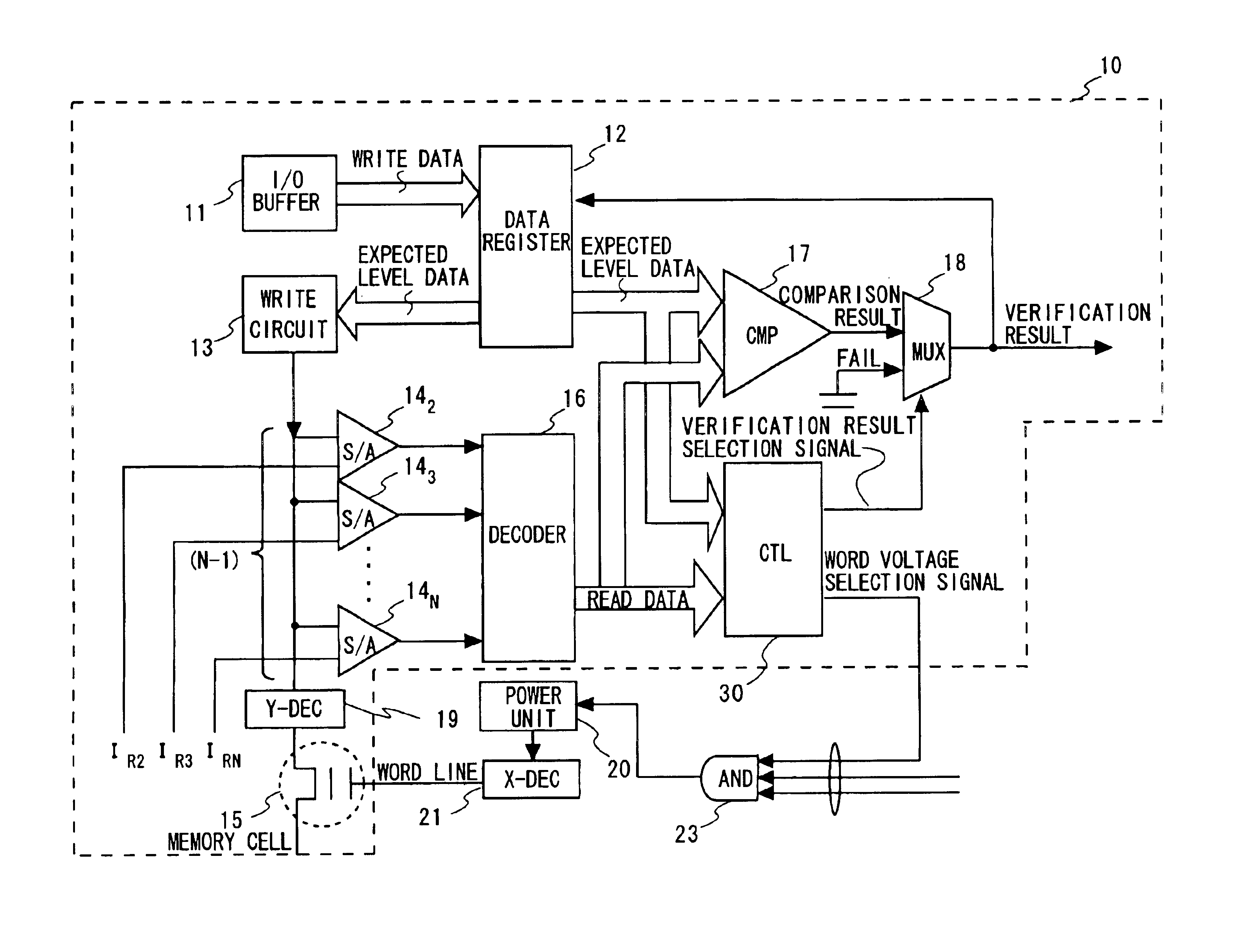
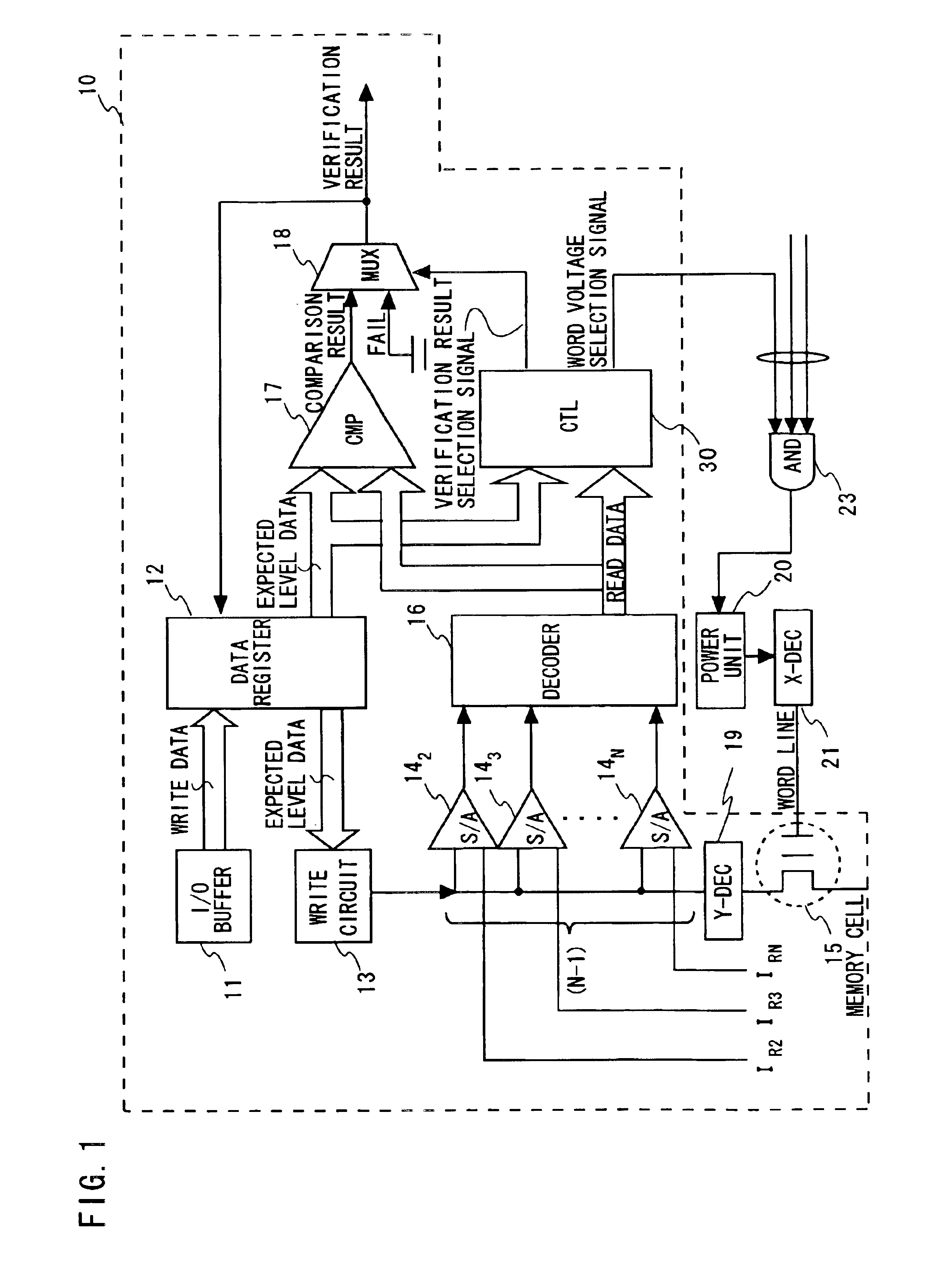
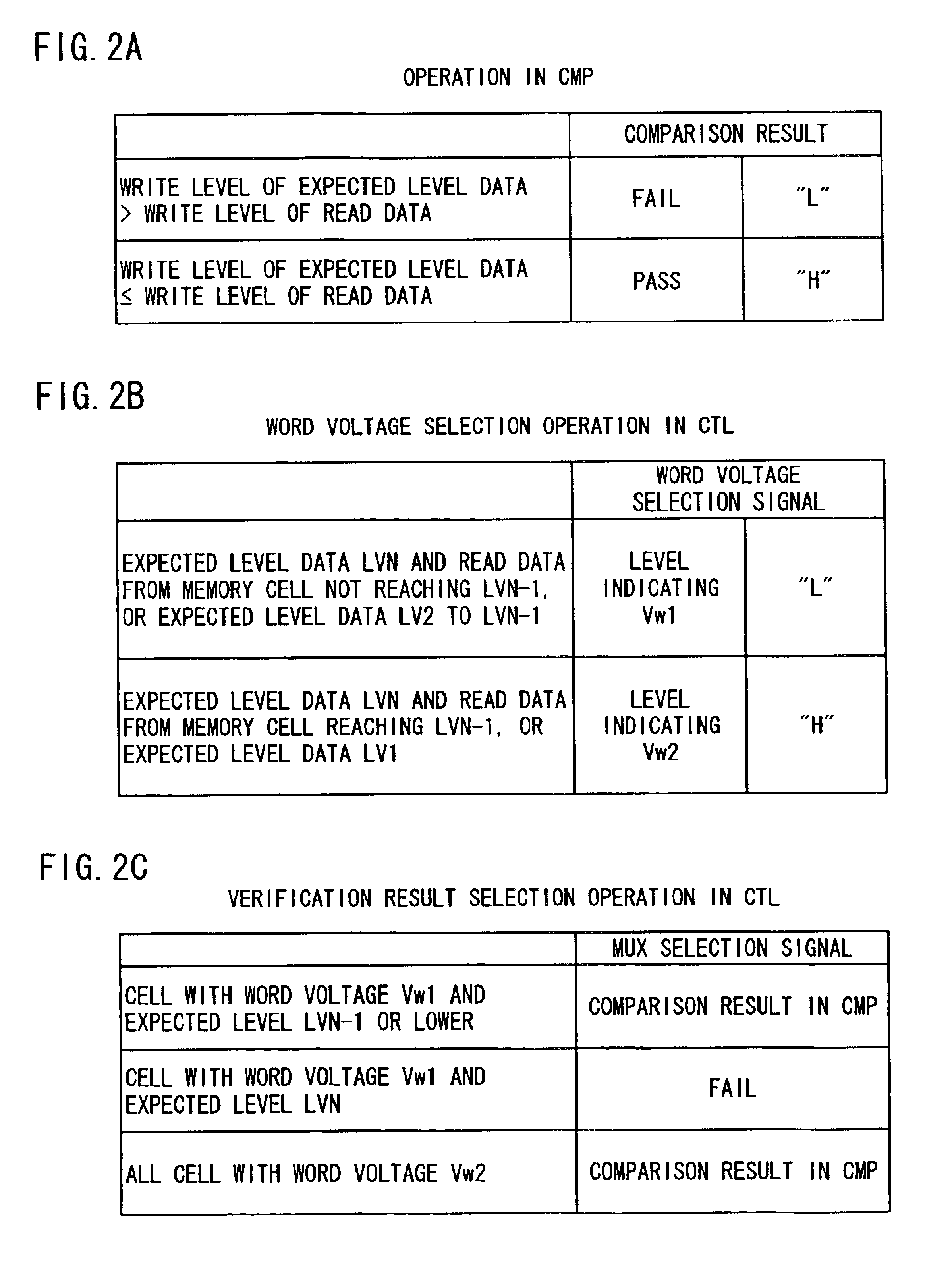
[0056]Referring to FIG. 1, it shows a block diagram showing an embodiment of a write circuit configuration for multilevel (N level; N≧3) nonvolatile semiconductor memory according to an embodiment of this invention. The data writing control circuits 100 encircled with a dotted line are provided to be of the same number as the number of the memory cells to which writing is performed simultaneously, as is the case with the configuration shown in FIGS. 6 and 7.

[0057]Each data writing control circuit 10 includes an I / O buffer 11 for inputting the write data specified by a user to a nonvolatile semiconductor memory cell 15 and outputting the stored data read out of the memory cell by the read operation. It also includes a data register 12 for holding the write data from the I / O buffer 11 and outputting the write data as expected level data, and a write circuit 13 for performing data writing to the nonvolatile semiconductor memory cell 15. Also included are sense amplifier 142 to 14N for ...


PUM


Abstract

In writing N level of multilevel data to nonvolatile semiconductor memory by repeating a verification process, a verification result of a memory cell where the Nth threshold level which is the highest level is to be written as an expected level is invalidated until completion of writing to a memory cell where the (N−1)th and lower level is to be written. The verification result of the memory cell where the Nth level is to be written is validated after reaching the (N−1)th write level. A reference current supplied to a sense amplifier corresponding to the Nth level is set at at least a level allowing no indeterminate sensing of a sense amplifier. In verification of the Nth level data, a word line voltage supplied for verify-reading is raised from VW 1 to VW 2.

Description

BACKGROUND OF THE INVENTION[0001]1. Field of the Invention[0002]The present invention relates to reprogrammable nonvolatile semiconductor memory devices such as EPROM and EEPROM, and more particularly, to a method for writing data to a multilevel cell able to store more than one bit of information in a single memory cell.[0003]2. Related Background Art[0004]A multilevel data storage nonvolatile semiconductor memory device which can store three or more levels of data (for example, four-level data: “00”, “01”, “10”, and “11”) in a single memory cell (EEPROM with NOR cell architecture) as a means to increase data density of reprogrammable nonvolatile semiconductor memory such as EPROM and EEPROM are disclosed in Japanese Unexamined Patent Application Publication No. H04-57294 and H10-302482, for example.[0005]Data writing to the multilevel nonvolatile semiconductor memory employing a data readout system that performs batch verification of N (N≧3) level data is generally performed as fo...

Claims


Application Information

Patent Timeline
Patent Type & Authority Patents(United States)
IPC IPC(8): G11C16/02G11C16/04G11C16/06G11C11/56G11C16/34
CPCG11C11/5628G11C16/3454G11C11/5642G11C2211/5621
Inventor FUNAKI, TOSHIHIKO
Owner RENESAS ELECTRONICS CORP
Why Eureka
Try Eureka