Optimal control of wide conversion ratio switching converters

Inactive Publication Date: 2005-09-06
MICROCHIP TECH INC
5 Cites 174 Cited by

AI-Extracted Technical Summary

Problems solved by technology

The result is extremely high operating temperature beyond the capability of standard power supplies containing electrolytic capacitors.
Further, light fixtures t...

Method used

[0035]Pin 2 of control circuit U1 is connected to a scaled and filtered signal proportional to the rectified AC input. U1 Pin 2 also controls the ON time of the MOSFET M1. By holding U1 pin 2 at a substantially constant voltage for a given AC input magnitude, the on time of the switch will be substantially constant and therefore for a relatively fixed switching frequency the average input current will be drawn in proportion with the input voltage—the result is high input power quality with PF>90% and THD<15%.
[0037]The control circuit in U1 produces independence between the feedforward and feedback sections of the circuit. The feedback maintains a substantially constant feedback voltage with C5& C8 in combination with resistor R1, R8 producing an optional low pass filter, which may not be needed depending upon the choice of compensation components C7& R2, the size of C3& L2, in conformance with the acceptable ripple in the load, 2. Resistor R3 is the sense resistor. The sense resistor voltage to be regulated may be chosen to be large in magnitude, such as −2.5V to escape the noise floor or alternatively may be chosen to be small such as −165 mV to save energy. An innovative feedback means which includes comparing the voltage developed across matched integrators, 214, does not require filtering of the feedback signal to close the loop.
[0040]Protection is provided in three forms. Firstly there is a thermal shutdown or limit circ...

Benefits of technology

[0016]In accordance with another embodiment of the present invention, the power supply circuit above is coupled to a feedback circuit. The feedback circuit comprises differential inputs wherein each terminal of the differential inputs is couple...

Abstract

A switch state controller generating a pulse train is used in a power converter utilizing a plurality of converter stages all simultaneously controlled by a single switch controlled by said pulse train. On time of the pulse train is controlled according to an input or interim node characteristic of the supply and period is controlled by a characteristic of the output of the converter. This allows development of AC-to-DC converters, including power-factor-correction converters, and DC to DC converters with high conversion ratio with minimal parts count & high reliability.

Application Domain

Efficient power electronics conversionApparatus without intermediate ac conversion +2

Technology Topic

Power factor correctorDC-to-DC converter +5

Image

  • Optimal control of wide conversion ratio switching converters
  • Optimal control of wide conversion ratio switching converters
  • Optimal control of wide conversion ratio switching converters

Examples

  • Experimental program(1)

Example

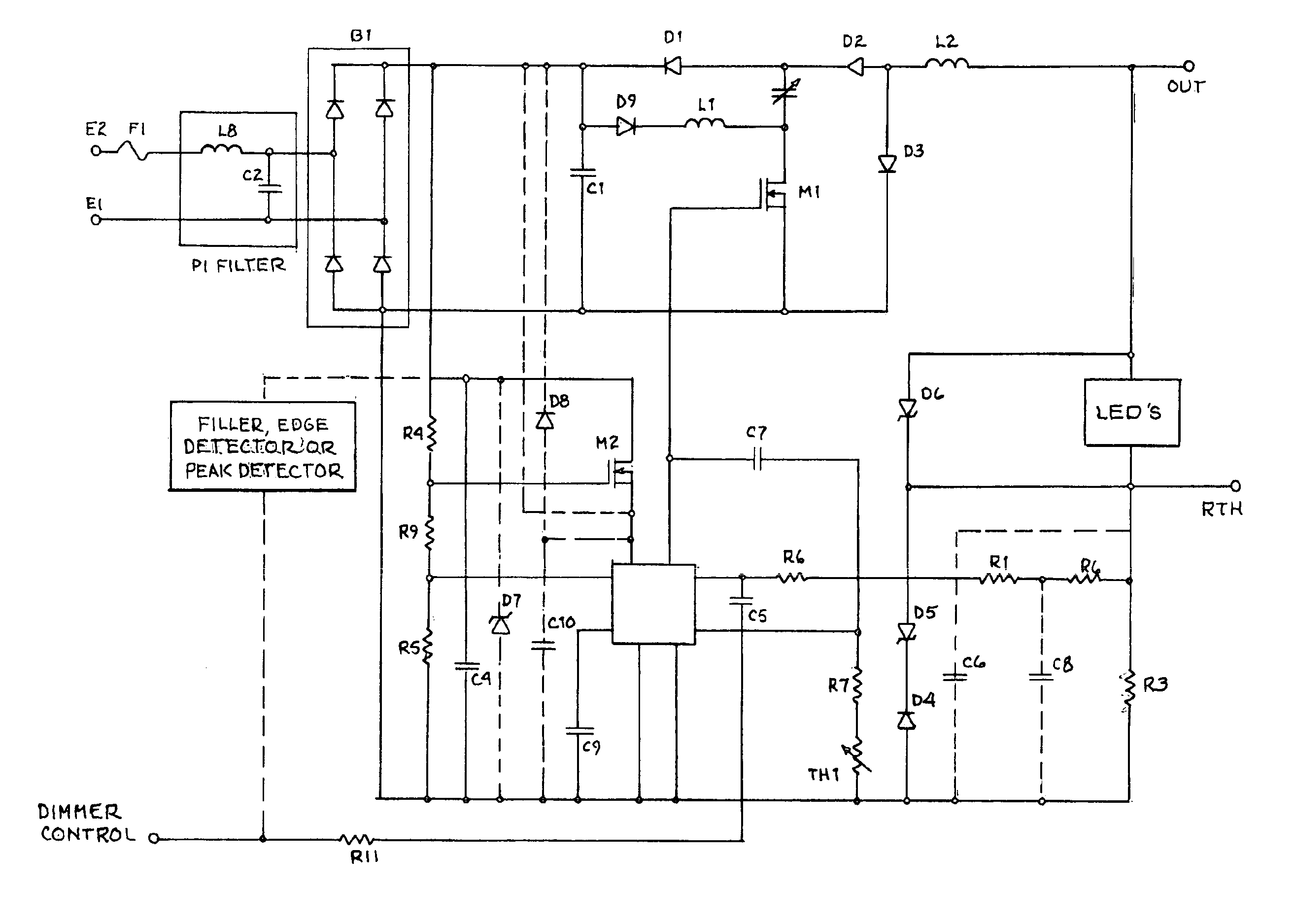
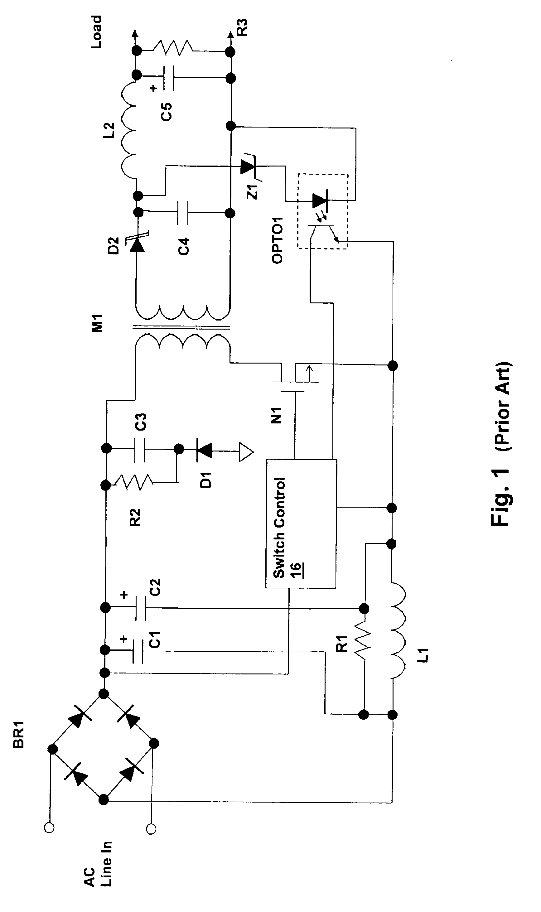
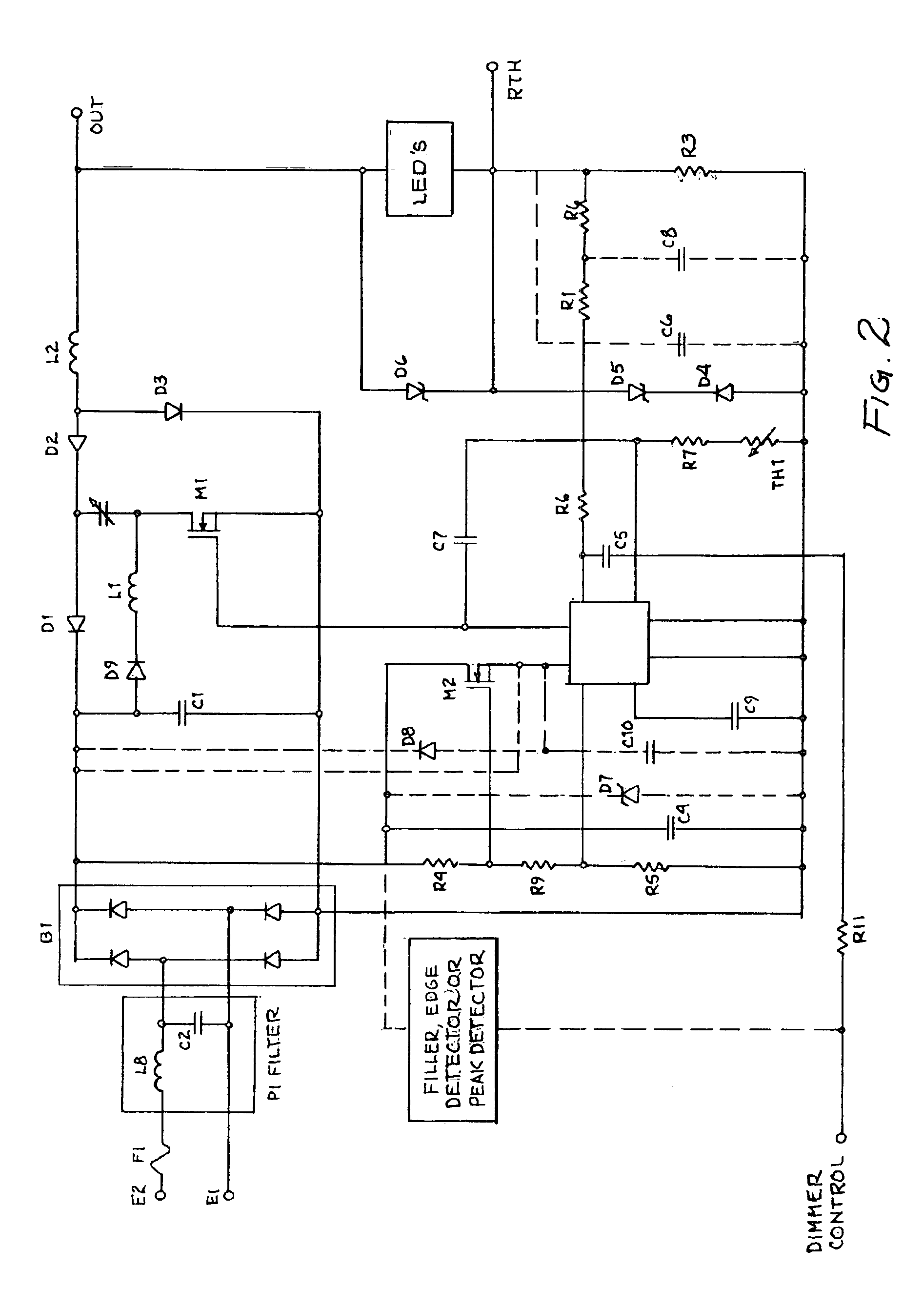
[0025]Referring to FIG. 1, a prior art power supply is depicted. A bridge BR1 full-wave rectifies an AC line input to produce an input power source. Filter capacitors C1 and C2 average the voltage at the output of bridge BR1 to produce a DC voltage (approximately 360 Volts DC without load). Without filter capacitors C1 and C2 the power supply cannot change control function (e.g., duty cycle in a pulse-width modulated (PWM) power supply) as the input waveform varies in voltage from 0V to 360V. The control function dynamic range required to accomplish proper line regulation, which is the power supply's rejection of input voltage variation, is too wide for operation without filtering. An inductor L1 is coupled between capacitors C1 and C2 to provide inrush protection and electromagnetic interference EMI filtering. A resistor R1 is used to set the initial inrush current, providing a soft-start current to charge capacitor C2 until the field produced in inductor L1 collapses.
[0026]The power supply of FIG. 1 is of typical design well-known in the art as a flyback converter. A transformer M1 couples energy from its primary side by the action of a switch implemented by a transistor N1. N1 is controlled by a switch control 16, typically a pulse-width modulator that varies duty cycle in conformity with a feedback signal provided from the circuit coupled to the secondary of transformer M1. A resistor R2, a capacitor C3 and a diode D1 form a “snubber” circuit that absorbs the current spike produced when transistor N1 is turned off that would otherwise produce a voltage spike on capacitor C2 (and a spike on capacitor C1 that will be reduced depending on the characteristics of inductor L1).
[0027]The secondary side of transformer M1 comprises a half wave rectifier implemented by a schottky diode D2 and a filter formed by capacitor C4 inductor L2 and capacitor C5. The filter removes the higher harmonics of the switching waveform (pulse) that is coupled from the primary side of transformer M1 to the secondary. A zener diode Z1 and optocoupler OPTO1 provide a feedback signal to switch control, so that the pulse width of the signal controlling the gate of transistor N1 may be varied to produce a constant voltage at capacitor C5 as load current and AC input voltage vary. A resistor R3 is coupled across the output terminals of the power supply (load terminals) and is generally necessary to produce a stable no-load operating point, but may be unnecessary in some implementations, where the minimum pulse width of the switch is sufficient to produce a stable no-load DC output.
[0028]The dynamic control range necessary to operate the power supply as described above without filter capacitors C1 and C2 is too wide for proper operation. For example, a 100 Khz PWM switch-mode power supply would have to produce a pulse width of 5 μs (50% duty cycle) at an input voltage of 0.67V and a pulse width of 5 ns (0.1% duty cycle) at an input voltage of 360V, in order to provide the equivalent performance of a filtered-input converter that can fully regulate it's control function on a pulse-by-pulse basis. Both the efficiency of such a power supply and the fast switching requirement at the low duty-cycle point make such a solution impractical. Further, present-day switch-mode power supplies typically switch at much higher frequencies, for example 1 Mhz, which exacerbates the above-described problem by a factor of ten.
[0029]Referring to FIG. 2 one embodiment of a power supply having a switch state controller (FIG. 3) is shown. E1& E2 are input terminals which may be coupled to an AC source, such as a pure AC signal, a phase controlled AC signal or other signal. The listing of the above should not be seen as to limit the scope of the present invention. L3& C2 are a conducted emissions filter meant to provide a high frequency path back to the power supply for high frequency signals it generates and to provide a high frequency impedance between the AC input and the power supply to block higher frequency signals generated by the power supply.
[0030]A rectifier device 1 couples the AC signal to the power supply input terminals. The power supply is a multiconverter. There are two converter stages switched by a single switching device, the switching device controlled by a controller integrated circuit 3. A buck second stage is shown but could be replaced by any second stage DC/DC converter.
[0031]The first converter stage has an input from the most positive terminal of the input rectifier and the drain of MOSFET M1. The second converter stage has an input from the anode of D1, cathode of D2 and negative terminal of C3 and the source of MOSFET M1.
[0032]C1 provides a low impedance path for high frequency signals associated with the switching of M1. There are two states, one when the switch M1 is ON and one when the switch M1 is OFF. During the ON state, inductor L1 and diode D9 are placed across the rectified AC voltage across the full bridge causing the current in L1 to rise at a rate of (Vbridge-VD9)L1. At the same time the voltage previously stored on C3 is placed across the load, 2, inductor L2, sense resistor, R3, and diode D2, causing the current to rise in L2 according to (VC3-Vload-VD2-VR3)/L2. During the OFF state, L1 transfers energy to C3 through D1 and D9. At the same time L2 freewheels through D3, sense resistor R3, and the load, 2.
[0033]Control circuit U1 may be connected directly across the rectified DC input, or may be connected as shown in FIG. 8. This connection uses M2 in a source follower configuration to provide undervoltage lockout and also to divide heating between M2 and U1. A resistor divider R4, R9& R5 is the reference for the source follower and is programmed such that the source of M2 will reach the under voltage lockout (UVLO) of the controller U1 at the desired UVLO threshold of the filtered rectified AC input. Alternatively if a higher effective UVLO than programmed into the integrated circuit, U1, is not needed and the integrated circuit package is thermally capable (the source follower transistor would otherwise handle a large portion of the thermal dissipation), then a high voltage regulator, 201, within the integrated circuit U1 may be connected directly across the rectified AC input without the need for follower means, M2. Another option is to reference the source follower, M2, to a specific voltage for example using a shunt device 5, so that the highest voltage rated capacitor which is not electrolytic (and therefore can operate at high temperatures), C6, may be connected to its source. A blocking device such as a diode coupled from this source D8, which is also coupled to the integrated circuit U1 regulator, 201, may then be coupled to the input of the power supply as a energy reservoir (power source) during the time that the rectified AC input falls below the capacitor voltage, C10. In such an instance an alternate signal conforming to the average or peak magnitude of the rectified AC input would need to be scaled and coupled to the Von, pin 2 of integrated circuit U1. In an alternative embodiment where the ON time is varied instantaneously with the rectified AC input voltage, this can reduce current spikes. In this embodiment it will reduce output filter requirements and reduce the size of the energy storage capacitor, C3.
[0034]An internal regulator coupled to pin 1 of U1 is internally coupled to C6 which stores energy to provide a powering mechanism for U1 during the time that the voltage on U1 pin 1 falls below the voltage on C6. C6 further provides a low impedance charge source to drive the switching MOSFET M1.
[0035]Pin 2 of control circuit U1 is connected to a scaled and filtered signal proportional to the rectified AC input. U1 Pin 2 also controls the ON time of the MOSFET M1. By holding U1 pin 2 at a substantially constant voltage for a given AC input magnitude, the on time of the switch will be substantially constant and therefore for a relatively fixed switching frequency the average input current will be drawn in proportion with the input voltage—the result is high input power quality with PF>90% and THD<15%.
[0036]The control circuit U1 includes a differential integrating feedback which works to achieve parity between two feedback currents flowing out of U1 pin 5 and U1 pin 6. To reach current parity it is necessary to produce a voltage at pin 5 such that Vpin5/(R7+Rth1) is equal to (Vpin6−VR3)/(R1+R6+R8). This programming method allows a pseudo-programmable sense voltage, across R3, to be selected as desired based on the above current balance. Rth1 illustrates that temperature dependent impedance devices such as an NTC or PTC may be used to adjust the feedback to provide the desired average current through the load at different temperatures.
[0037]The control circuit in U1 produces independence between the feedforward and feedback sections of the circuit. The feedback maintains a substantially constant feedback voltage with C5& C8 in combination with resistor R1, R8 producing an optional low pass filter, which may not be needed depending upon the choice of compensation components C7& R2, the size of C3& L2, in conformance with the acceptable ripple in the load, 2. Resistor R3 is the sense resistor. The sense resistor voltage to be regulated may be chosen to be large in magnitude, such as −2.5V to escape the noise floor or alternatively may be chosen to be small such as −165 mV to save energy. An innovative feedback means which includes comparing the voltage developed across matched integrators, 214, does not require filtering of the feedback signal to close the loop.
[0038]A capacitor C9 is connected across the differential input to provide a high frequency short. This is used to compensate for finite slew rates on the VCCS operational amplifiers which otherwise would cause a DC error (high frequency components within the bandwidth of the op amps but beyond its slew rates may have differing rise and fall slopes producing a net DC error after integration).
[0039]Compensation is achieved using C7 and R2 coupled between the gate output and the differential input of U1. If U1 is considered as a gain element from its differential input to the gate output, then it is easily seen that the C7 and R2 create a pole and a zero to allow compensation programming.
[0040]Protection is provided in three forms. Firstly there is a thermal shutdown or limit circuit with hysteresis, 222, to protect against die overtemperature. There is an internal shutdown logic or restart means if the internal VCO control register reaches an upper limit (ie. the loop does not close within the charge up time of the VCO register, 221). The third is an overvoltage clamp through D6 means which pulls additional current from the U1 pin 6 if the voltage across the load grows too large, to lower the frequency and quantity of energy transferred per cycle. D5 and D4 provide further overvoltage breakdown clamping if a fast overvoltage occurs more quickly than U1 is able to react.
[0041]The multiconverter topology, due to the storage element, C3, and elimination of a L1 discharge path to the input which would dissipate power, allows operation with a phase control signal, such as that produced by a typical wall dimmer. To use LED solid state lighting in retrofit applications it would be desirable if the LED drive signal were to dim and operate from such an input signal. The circuit in FIG. 8 will operate from such a signal if a peak detector, edge detector or averaging filter, 4, is coupled to the rectified AC input so that a signal proportional to the extent of phase change is communicated. This dimming signal may be coupled to U1 through a resistor, R11, for example and summed into the differential feedback to change the average load, 2, current to accomplish dimming. Whether operating from pure AC or from an phase controlled AC signal, the ripple through the load, 2, may be programmed to any desired level using one or more means including the choice of C3, the choice of compensation components C7& R2, a low pass filter coupled from the sense resistor, R3, to the differential feedback of U1, for example R1, C5, R8& C8, and/or through the use of an energy reservoir capacitor coupled to a follower, M2, and through a diode to the power supply input.
[0042]In certain LED applications, such as where Kelvin temperature and CRI must be maintained at certain levels, it is desirable to maintain a constant current profile in the LEDs. This constant current is not the average current, but rather the rise time and peak current operating in discontinuous mode. In other words a consistent current profile when current is flowing, even if current does not flow throughout the high frequency cycle. A second embodiment in which the load current, 2, waveform is measured, for example by coupling a measuring circuit to L2, whose peak current is maintained constant even while the average current varies to dim in L2 DCM, may be used to maintain a constant color spectrum, CRI & Kelvin temperature while dimming.
[0043]In certain applications, it may be desirable to further modify the operating characteristics of the converter in conformance with optically measured parameters and/or temperature. In such a circumstance a PTAT signal may be coupled to the differential feedback of U1 as may a signal proportional to a measured color or intensity. Such measurements may be made with an optical meter fabricated on the same integrated circuit as the switch state controller with an optical aperature provided in the integrated circuit package.
[0044]In certain applications it may further be desirable to mount solid state LEDs capable of replacing light sources, near to the AC/DC power supply with controller, to produce a form factor capable of retrofitting existing lighting sources. High power (>=1W) LEDs produce too much conducted heat for the use of conventional power supplies, which contain electrolytic capacitors, to operate for long periods of time in confined common lighting form factors, such as track fixtures, recessed downlights, or traffic light housings, etc. from which removal of heat is difficult.
[0045]Further, it is necessary to provide a mechanical means whereby the heat generated by LEDs and by the power supply may be conducted away to retain a reasonable operating temperature. Such a solution is possible using a multiconverter and controller, using the methods taught herein to eliminate the need for any electrolytic capacitors or components with short life at high temperatures (>90 C), and by using the same heatsink, such as an aluminum substrate PCB board, to couple heat away from both the LEDs and from the power supply.
[0046]Examples of retrofit solutions which would utilize a multiconverter & controller in close proximity with the LED source would include MR16 90% power factor, <15% THD), small size, long life at high temperature, and the 30% or less peak to average ripple desired in high power solid state LEDs such as the newly introduced Luxeon 1W or 5W White, Green, Amber, Blue & RED LEDs. The system would also be compatible with phase controlled AC dimming circuits commonly found in the incandescent electrical circuits likely to be targeted for solid state lighting retrofits to increase lamp life and efficiency.
[0047]While the invention has been particularly shown and described with reference to the preferred embodiments thereof, it will be understood by those skilled in the art that the foregoing and other changes in form, and details may be made therein without departing from the spirit and scope of the invention.

PUM

no PUM

Description & Claims & Application Information

We can also present the details of the Description, Claims and Application information to help users get a comprehensive understanding of the technical details of the patent, such as background art, summary of invention, brief description of drawings, description of embodiments, and other original content. On the other hand, users can also determine the specific scope of protection of the technology through the list of claims; as well as understand the changes in the life cycle of the technology with the presentation of the patent timeline. Login to view more.
Why Eureka
Try Eureka