Complementary metal oxide semiconductor image sensor and method of manufacturing the same

a metal oxide semiconductor and image sensor technology, applied in semiconductor devices, diodes, radiation control devices, etc., can solve the problems of reducing image quality, high production cost, and high cost of silicon substrate b>102/b>, so as to improve image quality, reduce production cost, and reduce image distortion.

Active Publication Date: 2005-09-13
AU OPTRONICS CORP
View PDF3 Cites 56 Cited by
  • Summary
  • Abstract
  • Description
  • Claims
  • Application Information

AI Technical Summary

Benefits of technology

[0011]It is therefore an object of the invention to provide a CMOS image sensor and method of manufacturing the same. By using a non-single-crystal-silicone-base substrate, the production cost can be reduced. In addition, using transparent gate electrodes instead of the polysilicon ones can solve the issue that a part of the incident light is absorbed by the polysilicon gate electrode in the art. Therefore, errors in the sensing result and the image distortion can be reduced, thereby improving the image quality.

Problems solved by technology

Since the silicone substrate 102 is very expensive, the production cost will be considerably high.
In addition, for a part of the incident light is absorbed by the polysilicon gate electrode 110, it will make an error on the sensing result and the sensing image to be distorted, thereby reducing the image quality.

Method used


Image

  • Complementary metal oxide semiconductor image sensor and method of manufacturing the same
  • Complementary metal oxide semiconductor image sensor and method of manufacturing the same
  • Complementary metal oxide semiconductor image sensor and method of manufacturing the same

Examples


Embodiment Construction

[0019]The invention provides a CMOS image sensor and method of manufacturing the same. By using a non-single-crystal-silicone-base substrate, the cost of fabricating can be reduced. In addition, forming transparent gate electrodes instead of the polysilicon ones in the image sensor can solve the issue that a part of the incident light will be absorbed by the polysilicon gate electrode in the art. Therefore, errors in the sensing result and the image distortion can be reduced, thereby the image quality is improved.

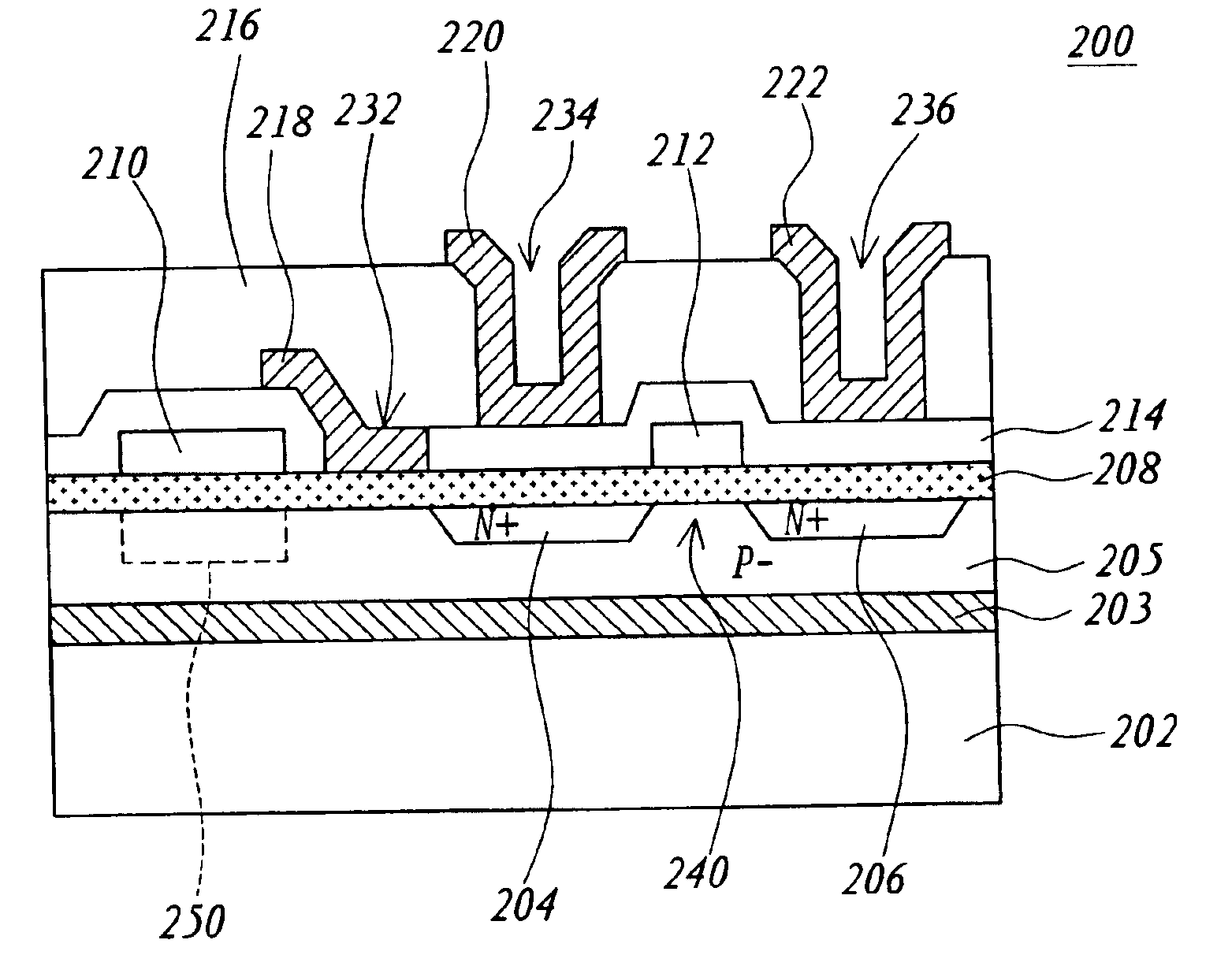
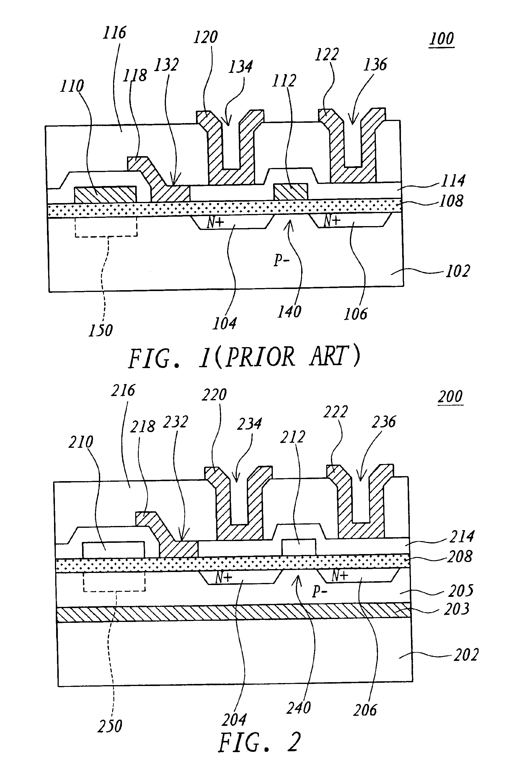
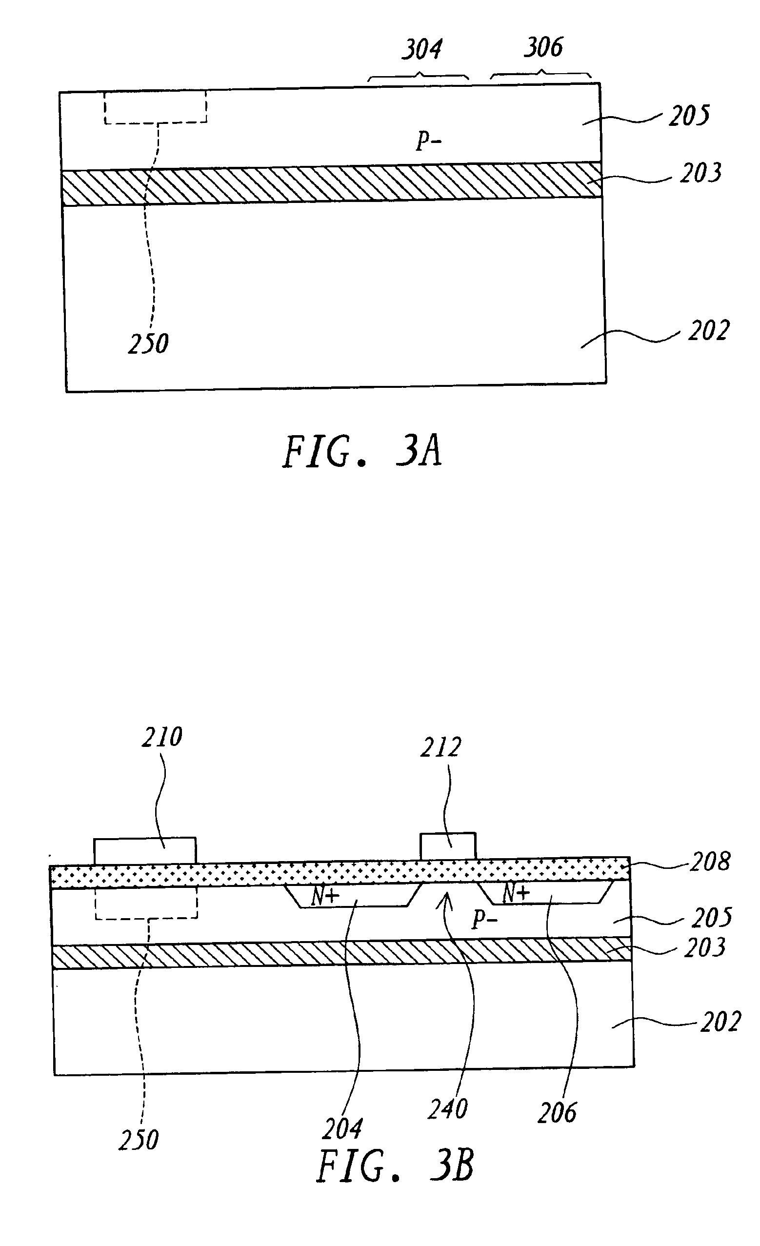
[0020]Referring to FIG. 2, a lateral view of a CMOS image sensor according to a preferred embodiment of the invention is shown. The CMOS image sensor 200 includes at least a non-single-crystal-silicone-base substrate 202, an opaque layer 203, a polysilicon layer 205, a source 204, a drain 206, a gate dielectric layer 208, transparent gate electrodes 210 and 212, an interlayer dielectric layer 214, a passivation layer 216, and metal electrodes 218, 220, and 222.

[0021]The opa...


PUM


Abstract

A complementary metal oxide semiconductor (CMOS) image sensor includes at least a non-single-crystal-silicone-base substrate, an opaque layer, a polysilicon layer, a source, a drain, a gate dielectric layer, a first transparent gate electrode, and a second gate transparent gate electrode. The opaque layer is formed on the non-single-crystal-silicone-base substrate, and the polysilicon layer, formed on the opaque layer, has a charge-generating region. The source and the drain are formed in the polysilicon layer, and a pre-channel region is formed between the source and the drain. The source is located between the pre-channel region and the charge-generating region. The gate dielectric layer is formed on the polysilicon layer, and the first and the second transparent gate electrodes, formed on the gate dielectric layer, are respectively located above the charge-generating region and the pre-channel region.

Description

[0001]This application claims the benefit of Taiwan application Serial No. 92112761, filed May 9, 2003.BACKGROUND OF THE INVENTION[0002]1. Field of the Invention[0003]The invention relates in general to a complementary metal oxide semiconductor (CMOS) image sensor and method of manufacturing the same, and more particularly to a CMOS image sensor, including a non-single-crystal-silicone-base substrate and transparent gate electrodes, and method of manufacturing the same.[0004]2. Description of the Related Art[0005]In the era of technology with rapid advances, image sensors have been widely applied in the fields of television, toys, security systems, scanners, mobile phones, digital video cameras, digital cameras, and many other portable electronic devices. Currently, there are at least two types of image sensors, which are a charge coupled device and a CMOS image sensor. Owing that CMOS image sensors can be mass-produced in semiconductor manufacturing process, their production costs ...

Claims


Application Information

Patent Timeline
Patent Type & Authority Patents(United States)
IPC IPC(8): H01L21/70H01L29/04H01L31/18H01L29/02H01L21/8238H01L31/036H01L31/00H01L31/0376H01L31/20H01L27/146
CPCH01L27/14601H01L27/14689H01L27/14643
Inventor YANG, CHIEN-SHENG
Owner AU OPTRONICS CORP
Why Eureka
Try Eureka