Input buffer circuit

a buffer circuit and input technology, applied in the field of input apparatus, can solve the problems of buffers operating and consuming electric power, circuits consuming current, and circuits consuming electric power even in standby sta

Active Publication Date: 2005-09-13
SK HYNIX INC
View PDF3 Cites 16 Cited by
  • Summary
  • Abstract
  • Description
  • Claims
  • Application Information

AI Technical Summary

Benefits of technology

[0010]Accordingly, the present invention has been made to solve the above-mentioned problems occurring in the prior art, and a first object of the present invention is to provide an input buffer circuit, in which a CMOS input apparatus operates in a predetermined operation (i.e. an input apparatus enables a CMOS buffer to operate when a refresh operation is performed), so as to prevent a differential buffer from operating and consuming electric power even without a command signal or an address signal inputted from an external.

Problems solved by technology

However, the conventional circuit as shown in FIG. 1 has a problem in that the circuit consumes a electric power even in a standby state.
That is, the buffers operate and consume electric power even in a predetermined time period for which the input apparatus does not operate.
For instance, even though an external command signal is not inputted while a refresh operation is performed, these input apparatuses (command and address buffer) are turned on, thereby consuming a current.
Further, when the reference potential Vref varies, these input apparatuses do not normally operate.
Herein, the reference potential Vref signal is changed into a ground potential, so that an abnormal operation may occur.

Method used


Image

  • Input buffer circuit
  • Input buffer circuit
  • Input buffer circuit

Examples


Embodiment Construction

[0027]Hereinafter, a preferred embodiment of the present invention will be described with reference to the accompanying drawings.

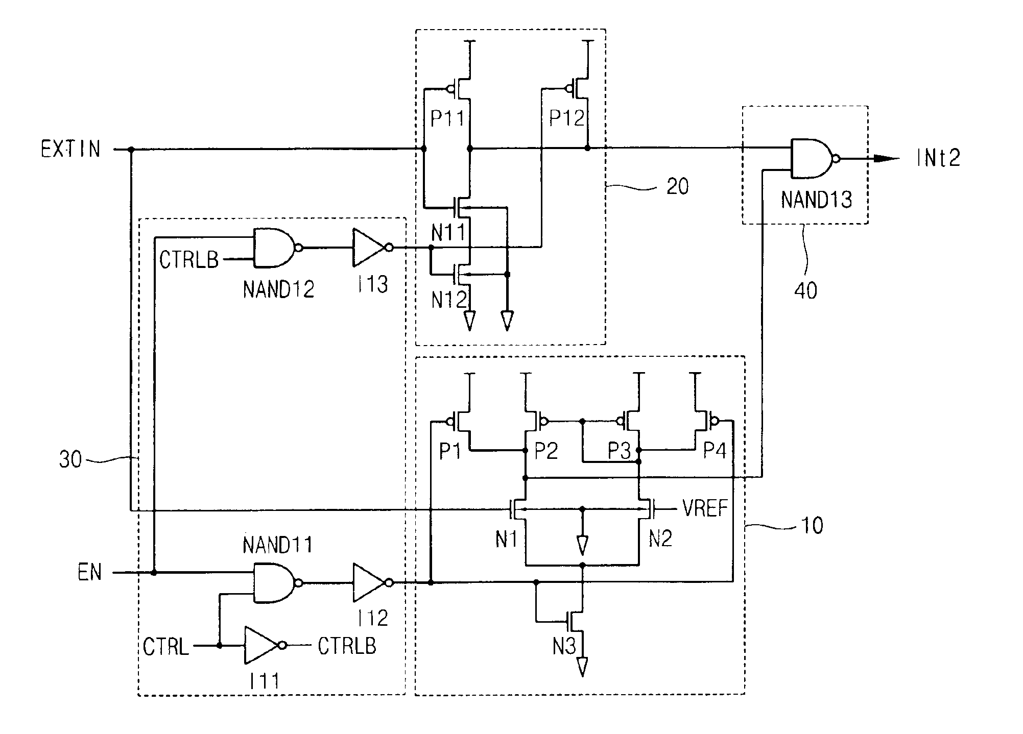
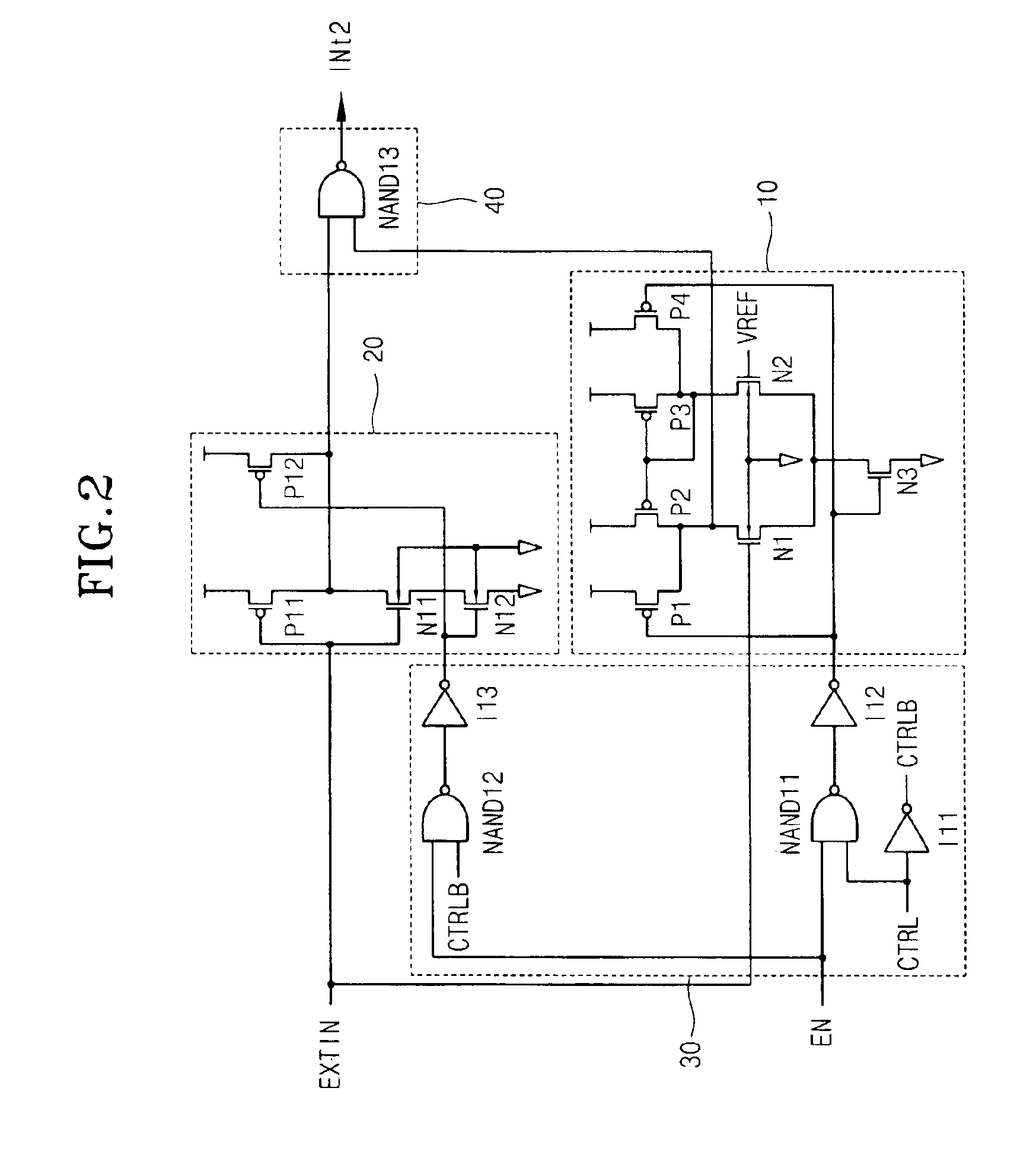
[0028]FIG. 2 is a circuit diagram of an input buffer according to the present invention.

[0029]The input buffer according to the present invention includes a differential buffer 10, a CMOS buffer 20, a control section 30, and an output section 40. The differential buffer 10 differentially compares a reference potential Vref with an external input signal EXTIN and buffers. The CMOS buffer 20 buffers the external input signal EXTIN. The control section 30 logically combines an enable signal EN inputted from an external and a control signal CTRL to operate the differential buffer 10 in a normal operation state in which the control signal CTRL is high, and operate the CMOS buffer 20 in a standby state in which the control signal CTRL is low. The output section 40 NANDs an output signal of the differential buffer 10 and an output signal of the CMOS buffer 20, an...


PUM


Abstract

Disclosed is an input apparatus used in a SSTL interface, which comprises a differential buffer for comparing an external input signal with a reference potential inputted from an external, and a CMOS buffer for buffering the external input signal. In the input apparatus, the CMOS buffer operates when a command signal or an address signal is not inputted from an external, and when a predetermined operation such as a refresh operation is performed, thereby reducing the power consumption in a standby mode. Further, in order to prevent the input apparatus from abnormally operating when the reference potential is not maintained in the normal operation range, a reference potential level detecting circuit is further included in the input apparatus, so that the CMOS buffer operates when the reference potential deviates from a predetermined normal operation range. Furthermore, in order to enable an input buffer to operate as the CMOS when an input signal fully swings, a circuit for detecting a potential of an input signal inputted from an external is further included in the input apparatus.

Description

BACKGROUND OF THE INVENTION[0001]1. Field of the Invention[0002]The present invention relates to an input apparatus used in a SSTL interface, and more particularly to an input buffer circuit having a differential buffer and a CMOS buffer as input buffers, which enables the CMOS buffer to operate in a predetermined operation such as a refresh operation, thereby preventing a current consumption from the input buffers in a standby mode and reducing the current consumption.[0003]2. Description of the Prior Art[0004]The SSTL interface enables a potential of a signal inputted from an external to move above or below a predetermined reference potential (e.g. 1.4V) with a variation within a predetermined potential (e.g. 0.4V), instead of moving between a source potential and a ground potential.[0005]A differential buffer circuit is mainly utilized as an input apparatus used in such a SSTL interface.[0006]FIG. 1 is a circuit diagram of an input buffer in a conventional SSTL interface. An exte...

Claims


Application Information

Patent Timeline
Patent Type & Authority Patents(United States)
IPC IPC(8): H03K19/00H03K19/018G11C7/10
CPCG11C7/1078H03K19/0016G11C7/1084G11C2207/2227H03K19/018
Inventor LEE, JAE JINLEE, KANG SEOL
Owner SK HYNIX INC
Why Eureka
Try Eureka