Optimum RF VCO structure

a voltage-controlled oscillator and optimal structure technology, applied in the direction of oscillation generators, pulse techniques, modulation, etc., can solve the problems of degrading vco performance, requiring additional area on the semiconductor, and additional cost, so as to reduce the area required on the semiconductor, increase the tuning range, and reduce the number of interconnections

Active Publication Date: 2005-09-13
NXP BV
View PDF1 Cites 23 Cited by
  • Summary
  • Abstract
  • Description
  • Claims
  • Application Information

AI Technical Summary

Benefits of technology

[0013]Systems and methods consistent with the present invention provide an optimal VCO implemention in a semiconductor that reduces the area required on the semiconductor for the VCO while reducing the number of interconnections and increasing the VCO's tuning range. At least two inductors are formed on the semiconductor material with one being formed offset in at least one of three dimensions from the other and both inductors having a common area enclosed by the at least two inductors. The common space within the at least two inductors is used for at least one electrical component.

Problems solved by technology

But such an approach requires additional area on a semiconductor wafer.
The additional area translates to additional cost and interconnections which degrade the VCO performance due to parasitic effects.
The drawbacks with such an implementation include the current losses that occur due to interconnections between capacitors / switches, the additional current loss caused by the switches or capacitors, and the increase in area that is required in a semiconductor chip having such an implementation.
The drawbacks with this implementation is the losses that occur due to interconnects between inductors / switches, the current losses within the switches and the additional inductors, as well as the increased space requirements on a semiconductor chip that incorporates such a VCO.

Method used


Image

  • Optimum RF VCO structure
  • Optimum RF VCO structure
  • Optimum RF VCO structure

Examples


Embodiment Construction

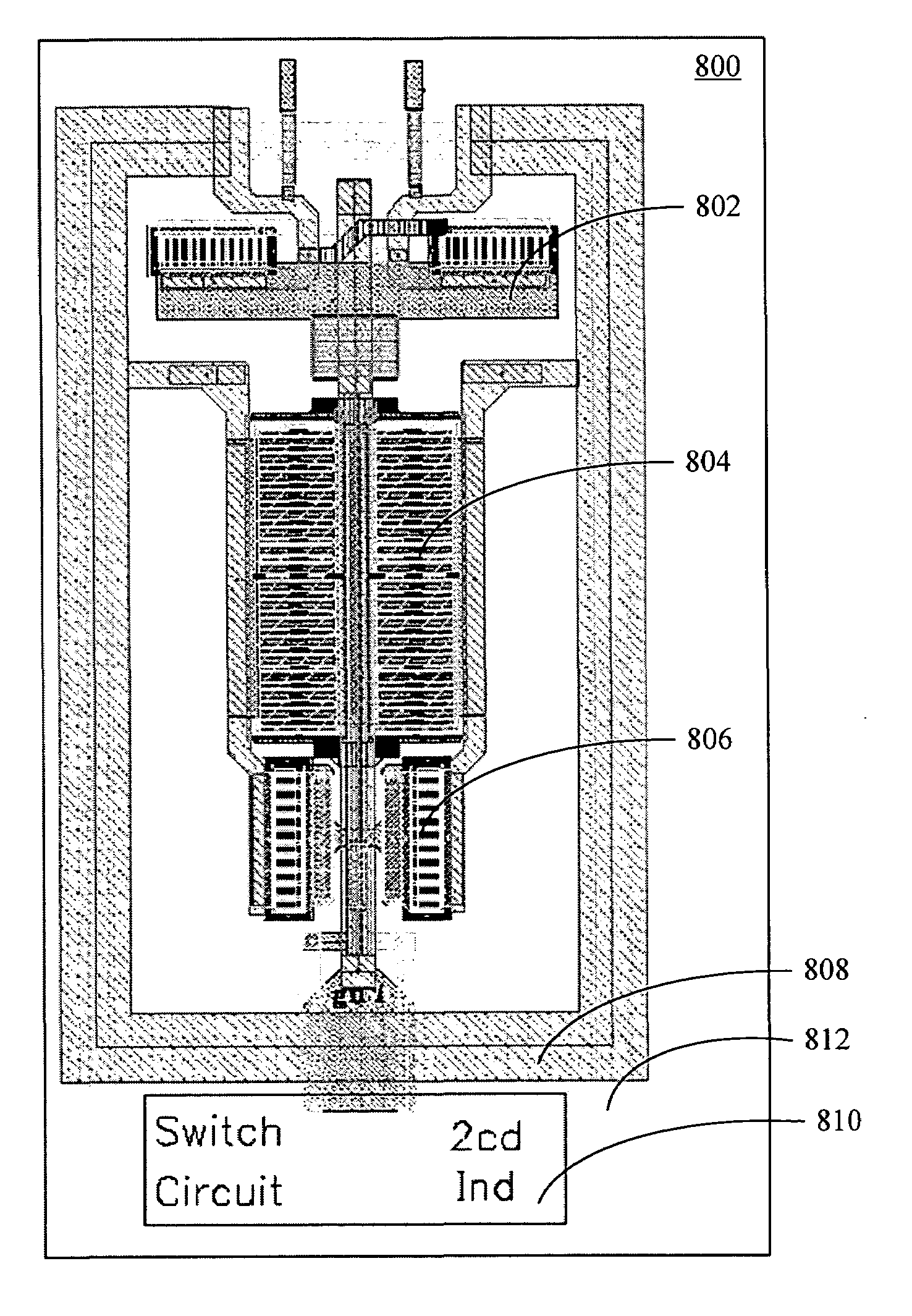
[0027]Turning to FIG. 6, that figure illustrates a circuit diagram for an RF voltage controlled oscillator (VCO) 600. The RF VCO may include a capacitor 602 connected in parallel with a varactor 604 by switch S1606. The varactor 604 is connected in parallel to inductor 608. A mutually coupled inductor 610 is switched into the RF VCO circuit by switch S2612. The switched-in mutually-coupled inductor 610 results in a band shift up in tuning range, while the switching in of capacitor 602 results in a shifting down of the tuning range.

[0028]An advantage of using the single inductive shift (i.e., the mutually-coupled inductor 610) is that the space in a semiconductor chip adjacent to the primary inductor or underneath the primary conductor in a multi-level metal layering process may be employed for the mutually conductive inductor. The placement of the mutually-conductive inductor results in a common area formed by the inductor and the mutually-conductive inductor. Such an area may then ...


PUM


Abstract

A voltage-controlled oscillator (VCO) formed upon a substrate with a first inductor being offset from a second inductor in one of three dimensions and forming a common area that may contain at least one of a varactor, capacitor, oscillator, or switch.

Description

BACKGROUND OF THE INVENTION[0001]1. Field of the Invention[0002]This invention relates generally to voltage-controlled oscillators, and more particularly to voltage-controlled oscillators formed in semiconductor material.[0003]2. Related Art[0004]Fixed frequency oscillators are typically devices formed out of semiconductor materials that generate an oscillating voltage in response to a direct current (DC) voltage being applied. Oscillators are often used as clocks in digital applications such as computers and signal sources in Radio Frequency (RF) applications such as cellular telephones. It is also known that combining a frequency selective network and an active device to sustain oscillation forms a fixed frequency oscillator. Turning to FIG. 1, a schematic diagram of a known fixed frequency oscillator 100 is illustrated. The schematic diagram 100 shows a frequency selective network 102 in electrical communication with an active device 104. The frequency selective network 102 may b...

Claims


Application Information

Patent Timeline
Patent Type & Authority Patents(United States)
IPC IPC(8): H03B5/08H03B5/12
CPCH03B5/1268H03B5/1243H03B5/1265
Inventor KALTENECKER, ROBERT S.
Owner NXP BV
Why Eureka
Try Eureka