Semiconductor device and its manufacturing method

a semiconductor device and manufacturing method technology, applied in the field of semiconductor devices, can solve the problems of increasing calorific power, deteriorating reliability, increasing power consumption of the entire semiconductor device, etc., and achieves the effects of preventing power consumption, preventing operating delays, and high-speed operation

Inactive Publication Date: 2005-09-20
SONY CORP
View PDF1 Cites 17 Cited by
  • Summary
  • Abstract
  • Description
  • Claims
  • Application Information

AI Technical Summary

Benefits of technology

[0013]In the semiconductor device of such a construction, because direct connection at the portion between the internal circuits of the semiconductor chips is established, in comparison with a case of connecting the internal circuits of the semiconductor chips via the external connection circuits thereof, power consumption in the external connection circuits is prevented, while, at the same time, operating delay between the semiconductor chips due to connection via the external connection circuits can be prevented.
[0014]Especially, by electrically cutting off the external connection circuits, which are drawn from the internal circuit connected to the other semiconductor chips, from the internal circuit, power supply to the cut off external connection circuits is stopped, hence, in the above-mentioned comparison, a further effect of preventing power consumption in the external connection circuits will become greater. A switch circuit for performing cut-off operation may be installed in each semiconductor chip.
[0018]As mentioned above, according to a semiconductor device of the present invention, by connecting directly between the portions of the internal circuits, while preventing power consumption in the external connection circuits, it becomes possible to prevent operating delay between the semiconductor chips otherwise caused by going through the external connection circuits, and thus it becomes possible to accomplish high-speed operation and low power consumption in a semiconductor device of the MCM type.
[0019]Further, according to a manufacturing method of a semiconductor device of the present invention, after completing the functional test of the internal circuits by using a sufficient number of the necessary external connection circuits, there is employed a construction in which direct connection is established between the semiconductor chips through the portions of the internal circuits. This makes it possible to obtain a semiconductor device having the semiconductor chips directly connected with the portions of the internal circuits without going through the external connection circuits used for the functional test while utilizing those semiconductor chips whose full reliability has been assured by the functional test.
[0020]Consequently, by using those semiconductor chips whose reliability has been assured, it becomes possible to obtain a semiconductor device of the MCM type which prevents extra power consumption in the external connection circuits as well as operating delay between the semiconductor chips otherwise caused by going through the external connections circuits.

Problems solved by technology

Since each of these circuits requires a very substantial quantity of current, an increase in power consumption of the entire semiconductor device is caused.
Such increase in power consumption leads to increasing calorific power in the semiconductor device, which in turn leads to deterioration of its reliability.
Further, connecting between the semiconductor chips 2 and 3 via the I / O circuit makes high-speed operation difficult.

Method used


Image

  • Semiconductor device and its manufacturing method
  • Semiconductor device and its manufacturing method
  • Semiconductor device and its manufacturing method

Examples


first preferred embodiment

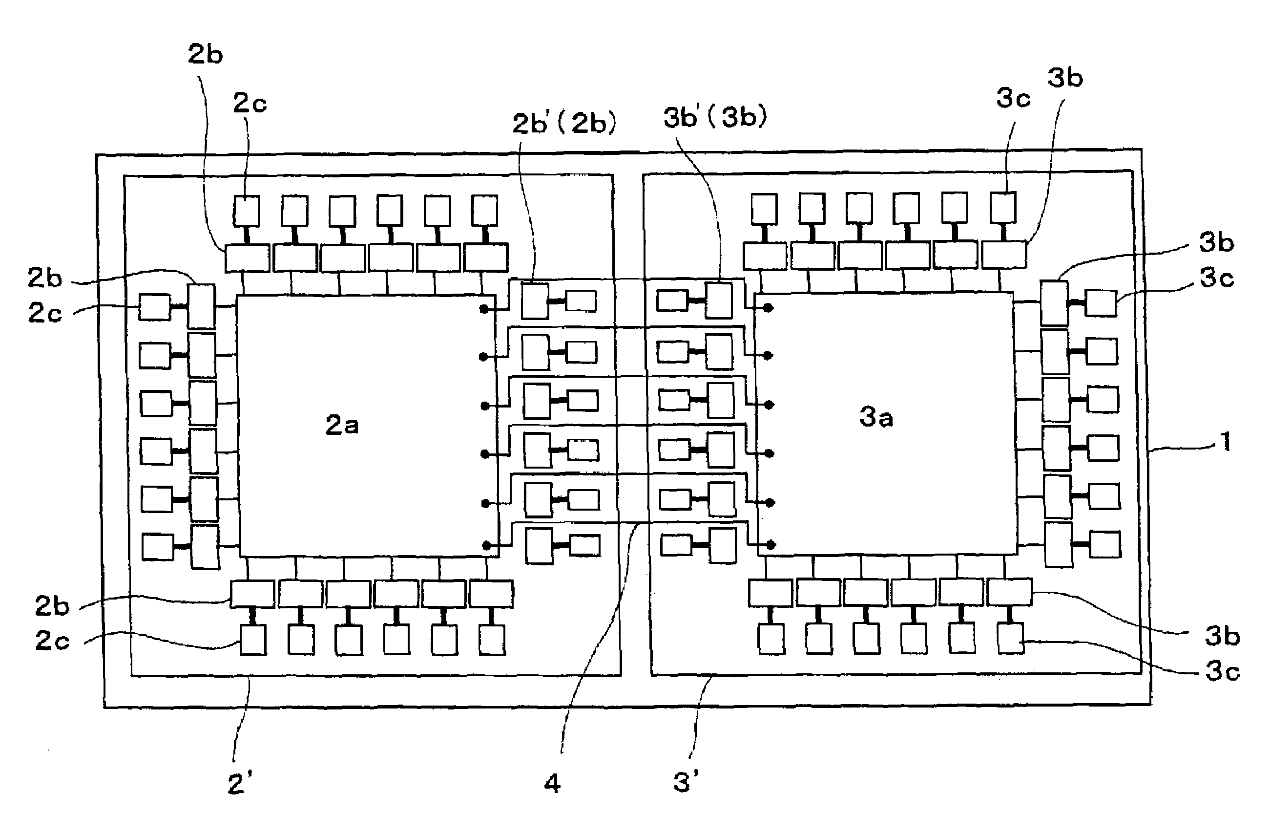
[0036]FIG. 1 is a plan view showing a first preferred embodiment of a semiconductor device according to the present invention.

[0037]The semiconductor device shown in this drawing is a semiconductor device of the so-called MCM type with a plurality of (two as illustrated) semiconductor chips 2 and 3 mounted on a supporting substrate 1.

[0038]The semiconductor chip 2 is a semiconductor chip for logic in which, as an internal circuit 2a, for example, a logic circuit for signal processing and a signal control circuit for reading an optical disk are formed. On the other hand, the semiconductor chip 3 is a semiconductor chip for memory in which as an internal circuit 3a, for example, a 32-bit, bus DRAM circuit is formed.

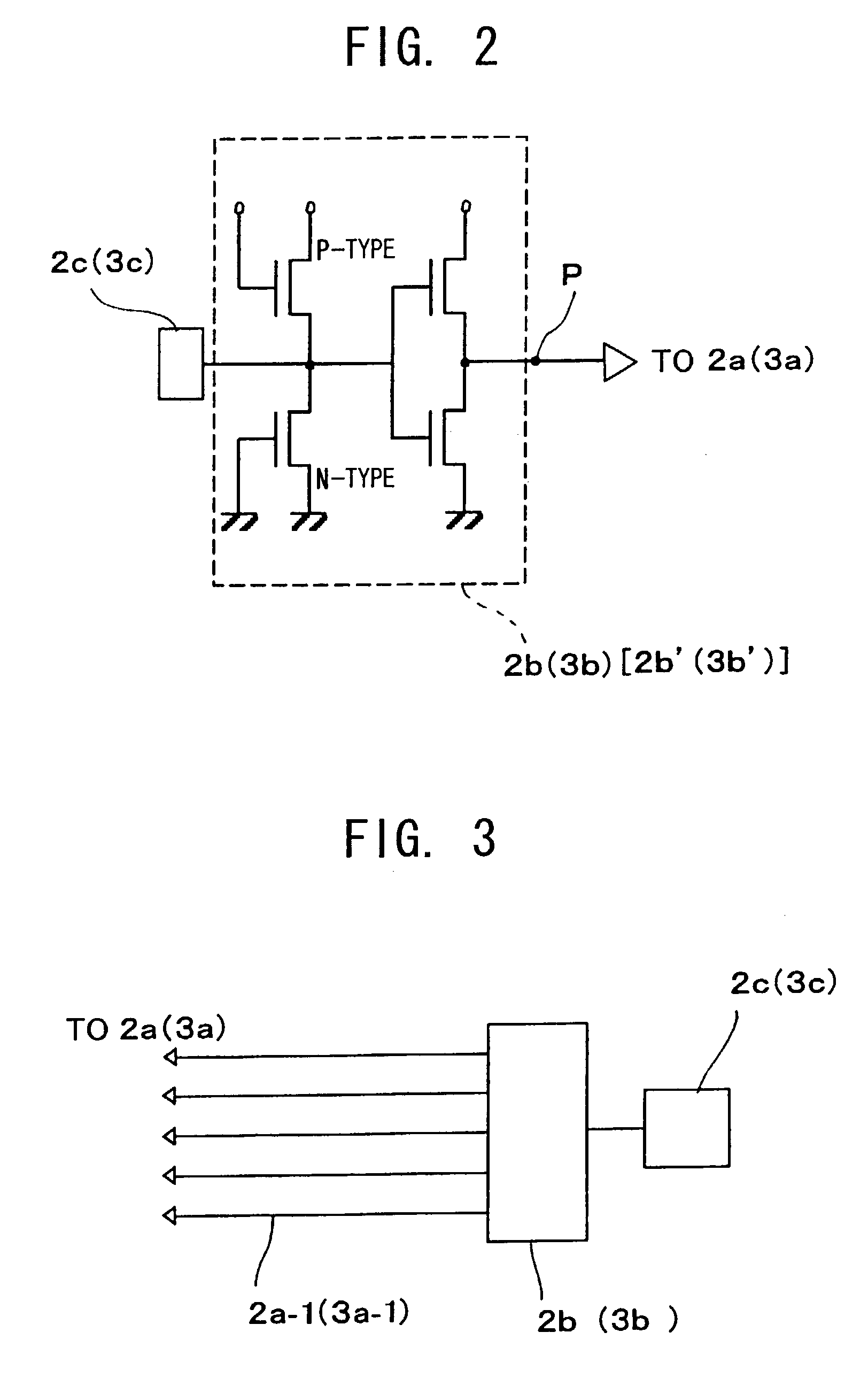
[0039]On these semiconductor chips 2 and 3, there are installed a plurality of external connection circuits 2b and 3b drawn from respective internal circuits 2a and 3a, and electrode pads 2c and 3c connected to each of these external connection circuits 2b and 3b. Each of t...

second preferred embodiment

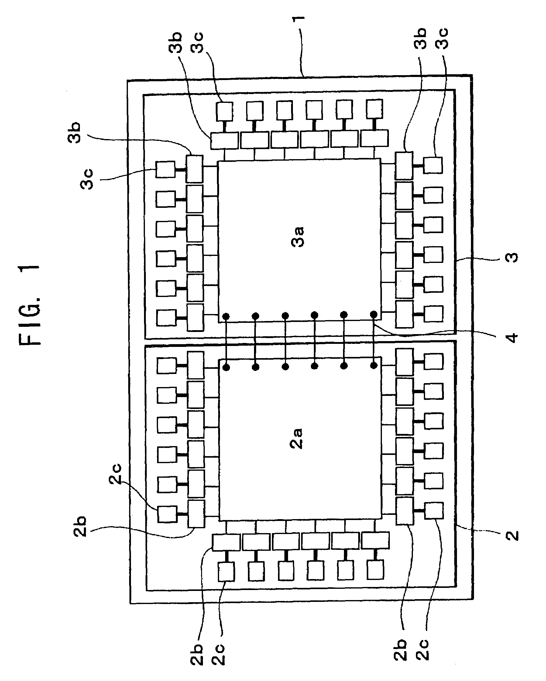
[0059]FIG. 6 is a plan view showing a second preferred embodiment of a semiconductor device according to the present invention. A difference between a semiconductor device illustrated in this drawing and a semiconductor device of a first preferred embodiment described by referring to FIG. 1 and FIG. 2 lies in a construction of semiconductor chips 2′ and 3′, construction of other parts being the same.

[0060]Namely, a characteristic feature of the semiconductor chips 2′ and 3′ used for the semiconductor device is that the external connection circuits 2b′ and 3b′ separated from the internal circuits 2a and 3a remain as they are on the semiconductor chips 2′ and 3′. In other words, of the external connection circuits 2b and 3b, those portions of the external connection circuits 2b′ and 3b′ drawn from the portions of the internal circuits 2a and 3a which are connected to other semiconductor chips 2 and 3 on the supporting substrate 1 are electrically cut off from the internal circuits 2a ...

third preferred embodiment

[0070]FIG. 7 is a plan view showing a third preferred embodiment of a semiconductor device according to the present invention. A difference between a semiconductor device illustrated in this drawing and the semiconductor device of the first preferred embodiment described by referring to FIG. 1 lies in a construction of a part of the external connection circuits set up on semiconductor chips 2″ and 3″.

[0071]Namely, on the semiconductor chips 2″ and 3″ used for the present semiconductor device, there are set up external connection circuits 2b and 3b similar to those described in the first preferred embodiment and the second preferred embodiment. Also, on those portions drawn from the portions of the internal circuits 2a and 3a connected to the other semiconductor chips 2″ and 3″ which are mounted on the supporting substrate 1, there are set up external circuits 6a and 6b, each provided with an external connection circuit and a separating circuit. Further, by means of the wiring 4 set ...


PUM


Abstract

A semiconductor device of the MCM type capable of high-speed operation and low power consumption and its manufacturing method are provided. A plurality of semiconductor chips, each having an internal circuit as well as an external connection circuit drawn from the internal circuit, are mounted on the same supporting substrate of this semiconductor device. Semiconductor chips are connected with each other, not by way of the external connection circuits, but directly at a portion between the internal circuits through wiring. This wiring is patterned on an insulating film provided on the supporting substrate and covers the semiconductor chips. Accordingly, through connection holes formed on the insulating film, connection can be established to the internal circuits or the wiring can be formed on the supporting substrate side. If the wiring is formed on the supporting substrate side, the semiconductor chips are to be mounted facing down relative to the supporting substrate.

Description

CROSS REFERENCES TO RELATED APPLICATIONS[0001]The present document is based on Japanese Priority Documents JP 2002-067969, JP 2002-236348 and JP 2002-327852, filed in the Japanese-Patent Office on March 13, August 14 and Nov. 12, 2002, respectively, the entire contents of which being incorporated herein by reference.BACKGROUND OF THE INVENTION[0002]1. Field of the Invention[0003]The present invention relates to a semiconductor device and its manufacturing method, and, more particularly, to a semiconductor device subjected to the application of so-called multi-chip module techniques, in which a plurality of semiconductor chips are incorporated as one electronic component, and its manufacturing method.[0004]2. Description of the Related Art[0005]To meet the demands of miniaturized lightweight, and low-energy consumption electric and electrical products, together with the high integration technology of semiconductor chips, packaging techniques to mount these semiconductor chips in high...

Claims


Application Information

Patent Timeline
Patent Type & Authority Patents(United States)
IPC IPC(8): H01L23/48H01L29/40H01L23/52H01L25/04H01L25/18H01L25/065H01L27/10
CPCH01L25/0655H01L25/0657H01L2224/16145H01L2224/16225H01L2224/73207H01L2924/15192H01L2924/15311H01L2224/0401H01L2224/04042H01L2224/16227H01L2924/19107H01L23/12
Inventor MORI, YUKARIEZAKI, TAKAYUKIHIRAYAMA, TERUOSASAKI, NAOTOOZAKI, HIROSHIISHIKAWA, NATSUYA
Owner SONY CORP
Why Eureka
Try Eureka