
Compact balun for rejecting common mode electromagnetic fields

a technology of electromagnetic fields and compact baluns, applied in the field of waveguides, can solve the problems of unsatisfactory low for many dds applications, large ferrite baluns are difficult to incorporate into miniature dds integrated circuits, and ferrite baluns are more suitable for continuous wave applications and less suitable for pulse applications. , to achieve the effect of facilitating load matching, novel design and facilitating the implementation of present invention

Inactive Publication Date: 2005-09-20
RAYTHEON CO
View PDF6 Cites 8 Cited by
  • Summary
  • Abstract
  • Description
  • Claims
  • Application Information

AI Technical Summary

Benefits of technology

The solution provides a miniature, wideband balun that efficiently rejects common mode energy and achieves broadband performance from multi-megahertz to multi-gigahertz frequencies, suitable for integration into DDS systems, improving signal-to-noise ratio and reducing phase noise.

Problems solved by technology

Unfortunately, ferrite baluns are bandlimited at lower frequencies, typically cutting off frequencies beyond two or three gigahertz, which is undesirably low for many ΔΣ DDS applications.
Furthermore, ferrite baluns are more suitable for continuous wave applications and less suitable for pulse applications, as ferrite baluns are often susceptible to reflections resulting from fast input pulses.
The large ferrite baluns are difficult to incorporate into miniature ΔΣ DDS integrated circuits and poorly reject common mode energy.
Unfortunately, use of quarter wavelength sections may result in undesirably large baluns.
In addition, these baluns are relatively narrow-banded and are susceptible to large reflections when fed with pulsed inputs.

Method used


Image

  • Compact balun for rejecting common mode electromagnetic fields
  • Compact balun for rejecting common mode electromagnetic fields
  • Compact balun for rejecting common mode electromagnetic fields

Examples


Embodiment Construction

[0021]While the present invention is described herein with reference to illustrative embodiments for particular applications, it should be understood that the invention is not limited thereto. Those having ordinary skill in the art and access to the teachings provided herein will recognize additional modifications, applications, and embodiments within the scope thereof and additional fields in which the present invention would be of significant utility.

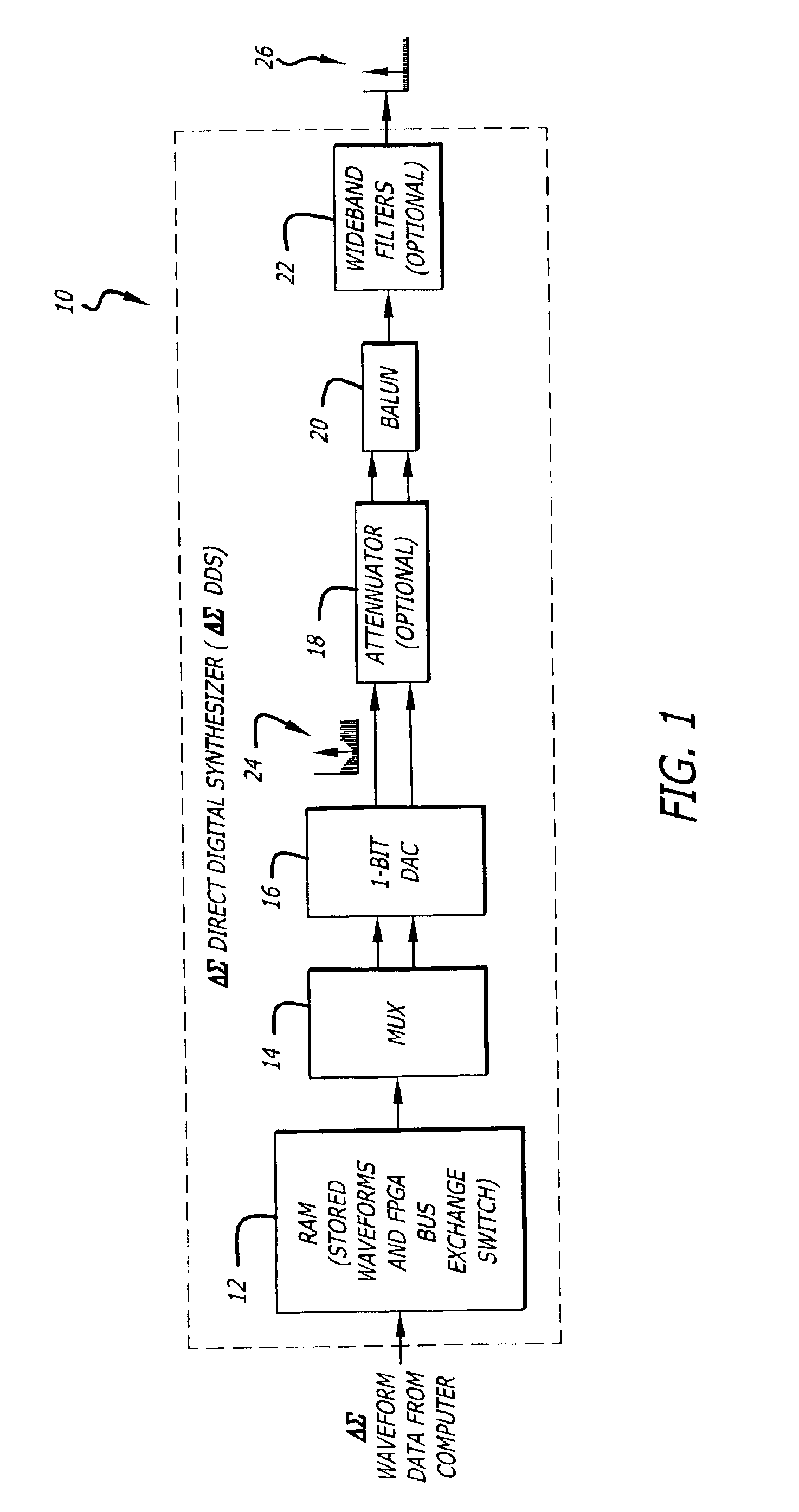
[0022]FIG. 1 is a diagram of a ΔΣ DDS 10 employing a compact broadband balun 20 that is constructed in accordance with the teachings of the present invention. For clarity, various well-known components, such as power supplies, clocking circuitry, software feedback loops, and so on, have been omitted from the figures. However, those skilled in the art with access to the present teachings will know which components to implement and how to implement them to meet the needs of a given application.

[0023]The ΔΣ DDS 10 includes, from left to ...


PUM


Abstract

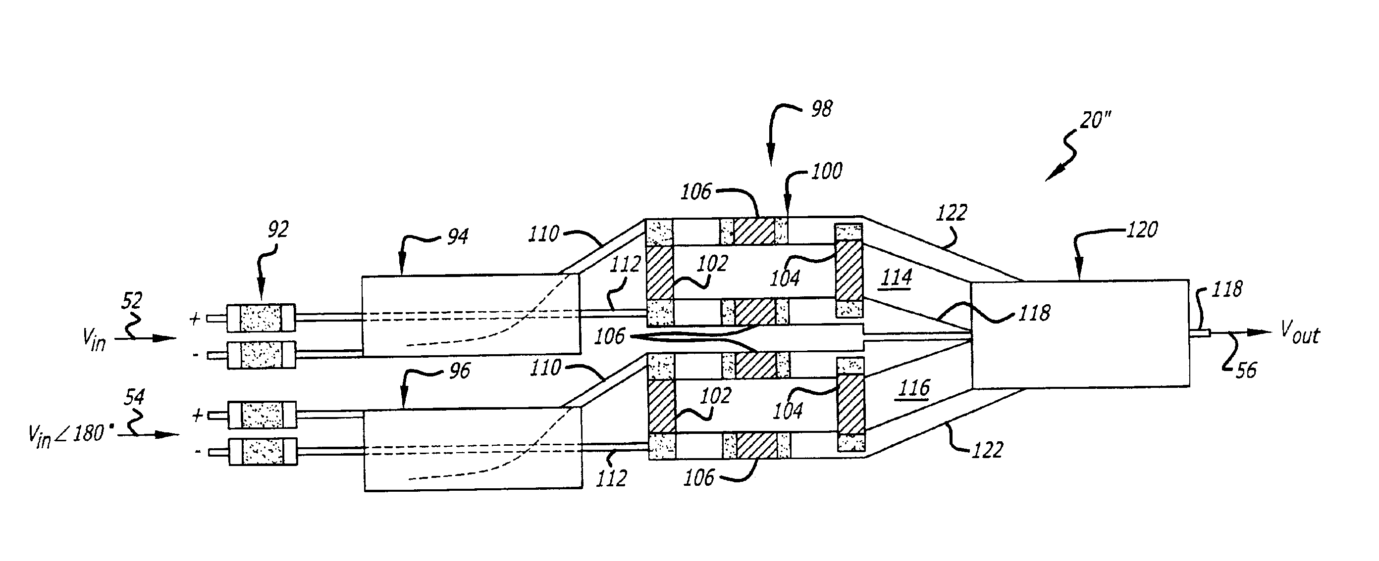
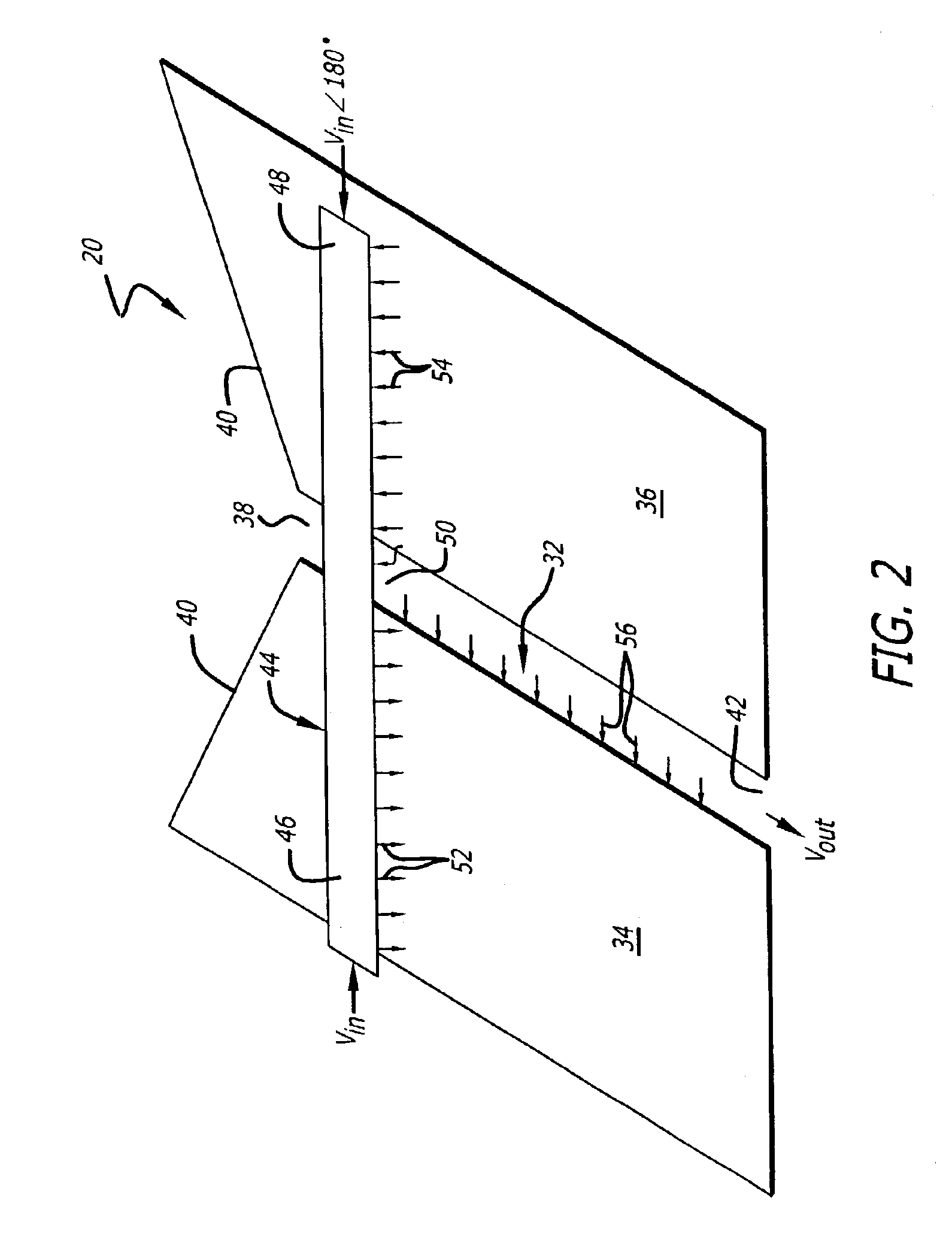
A space-efficient broadband balun (20). The balun (20) includes a first mechanism (44, 80, 82, 94, 96) for receiving an input signal (52, 54) having an undesirable component. A second mechanism (50) rejects the undesirable component via a waveguide transition (50). In a specific embodiment, the undesirable component is a common mode component. The first mechanism (44) includes an input microstrip waveguide (44). The waveguide transition (50) is a single microstrip-to-slotline transition (50) from the input microstrip waveguide (44) and to a slotline (32) in a ground plane (34, 36) of the microstrip waveguide (44). The slotline (32) is terminated at a first end (38) via a wedge (40) in the ground plane (34, 46). A second end (42) of the slotline (32) provides an output of the balun (20). The input signal (52, 54) includes a first input signal (52) and a second input signal (54), which are input at opposite ends (38, 42) of the input microstrip waveguide (44). The first input signal (52) and the second input signal (54) have a desired differential mode component and an undesired common mode component.

Description

BACKGROUND OF THE INVENTION[0001]1. Field of Invention[0002]This invention relates to waveguides. Specifically, the present invention relates to baluns for canceling common mode electromagnetic energy in differential input signals or for providing differential output signals lacking common mode energy in response to an input signal.[0003]2. Description of the Related Art[0004]A balun converts unbalanced transmission line inputs into one or more balanced transmission line outputs or visa versa. Baluns are employed in various demanding applications including output stages of delta sigma modulator Direct Digital Synthesizers (ΔΣ DDS) and antenna feeds. Such applications demand miniature, wide-bandwidth (wideband) baluns compatible with integrated circuits and capable of rejecting common mode energy from differential inputs or providing differential outputs lacking common mode energy.[0005]Space-efficient, wideband baluns are particularly important in ΔΣ DDS applications, where dual wid...

Claims


Application Information

Patent Timeline
Patent Type & Authority Patents(United States)
IPC IPC(8): H01P5/10
CPCH01P5/10
Inventor ESSENWANGER, KENNETH ALAN
Owner RAYTHEON CO
Learn More