Method and apparatus for optically aligning integrated circuit devices

a technology of integrated circuit devices and optical alignment, which is applied in the testing/measurement of individual semiconductor devices, semiconductor/solid-state devices, instruments, etc., can solve the problems of insufficient accuracy of aligning semiconductor chips, affecting the accuracy of alignment, and causing bottlenecks. achieve the effect of convenient alignmen

Active Publication Date: 2005-09-27
ORACLE INT CORP
View PDF8 Cites 29 Cited by
  • Summary
  • Abstract
  • Description
  • Claims
  • Application Information

AI Technical Summary

Benefits of technology

[0011]One embodiment of the present invention provides a system that facilitates aligning a first semiconductor die with a second semiconductor die, wherein the first semiconductor die and the second semiconductor die are arranged active face to active face. Note that the active face contains circuitry for communicating between semiconductor dies. The system starts by generating light on an active face of the first semiconductor die. The system then collimates the light within the active face of the first semiconductor die to form a first beam of light which is projected onto the second semiconductor die. Next, the system receives the first beam of light on an active face of the second semiconductor die and determines a position of the first beam of light on the active face of the second semiconductor die. Finally, the system determines an alignment of the second semiconductor die relative to the first semiconductor die based on the determined position of the first beam of light.

Problems solved by technology

Unfortunately, these advances in semiconductor technology have not been matched by corresponding advances inter-chip communication technology.
This problem is beginning to create a bottleneck that continues to grow as semiconductor integration densities continue to increase.
However, it is not a simple matter to align semiconductor chips with sufficient accuracy to facilitate chip-to chip communication.

Method used


Image

  • Method and apparatus for optically aligning integrated circuit devices
  • Method and apparatus for optically aligning integrated circuit devices
  • Method and apparatus for optically aligning integrated circuit devices

Examples


Embodiment Construction

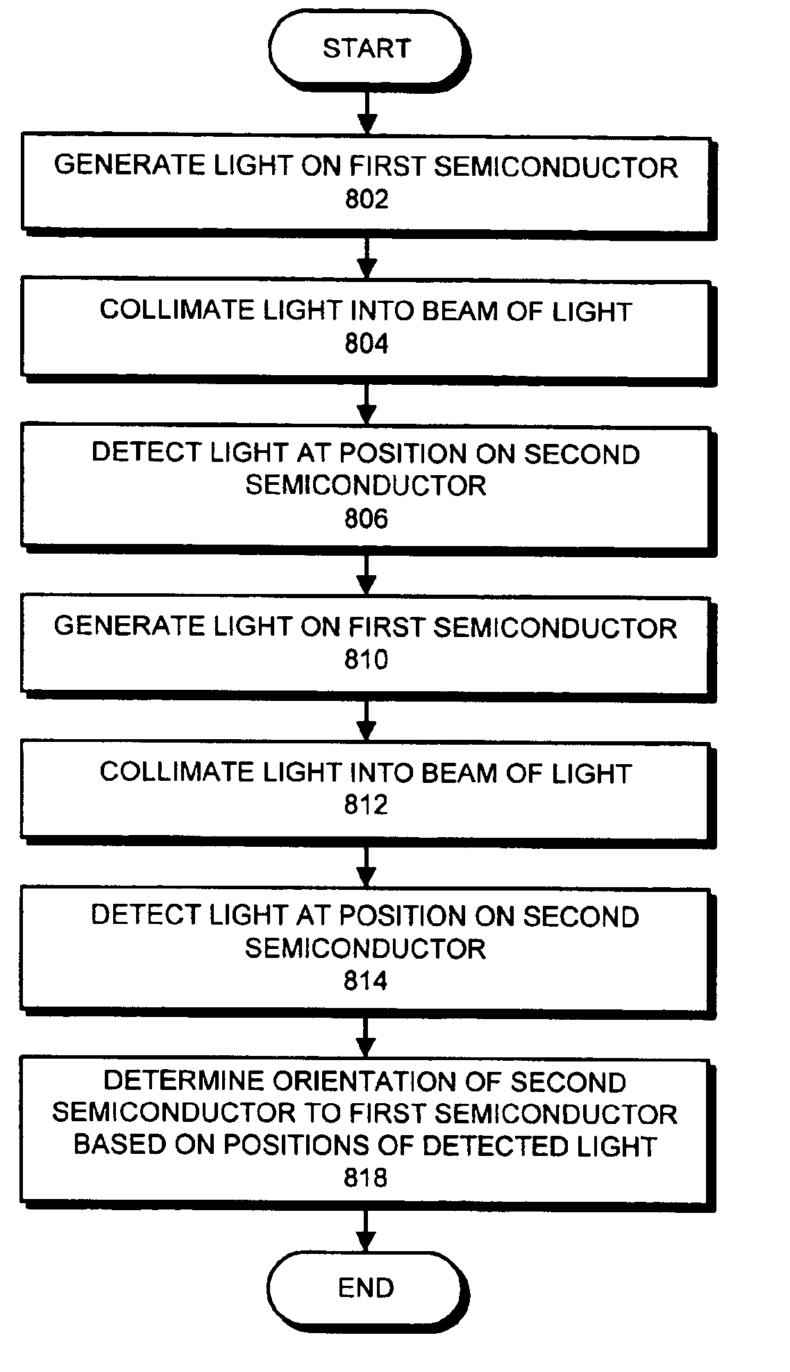
[0032]The following description is presented to enable any person skilled in the art to make and use the invention, and is provided in the context of a particular application and its requirements. Various modifications to the disclosed embodiments will be readily apparent to those skilled in the art, and the general principles defined herein may be applied to other embodiments and applications without departing from the spirit and scope of the present invention. Thus, the present invention is not intended to be limited to the embodiments shown, but is to be accorded the widest scope consistent with the principles and features disclosed herein.

Semiconductor Dies

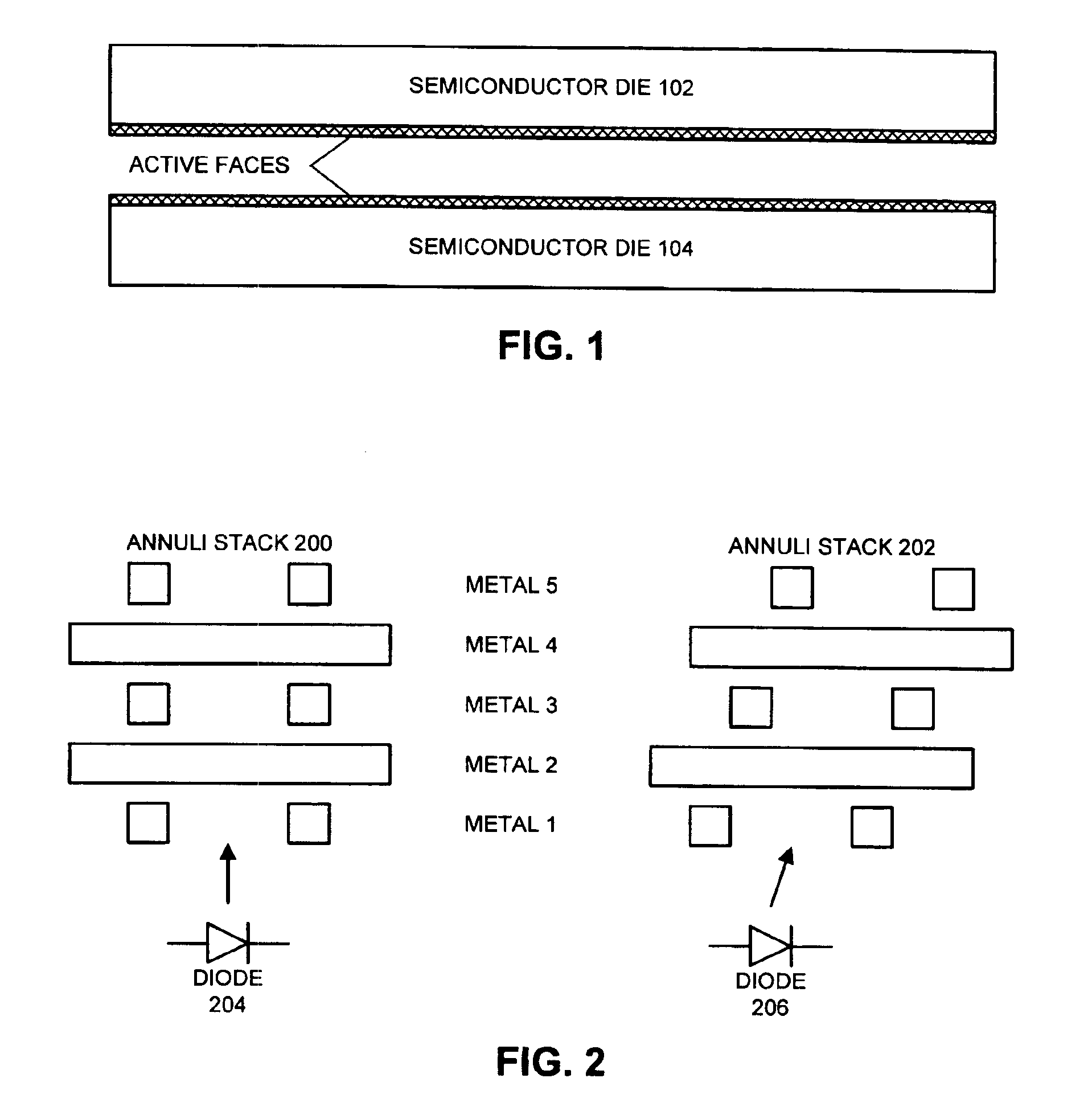
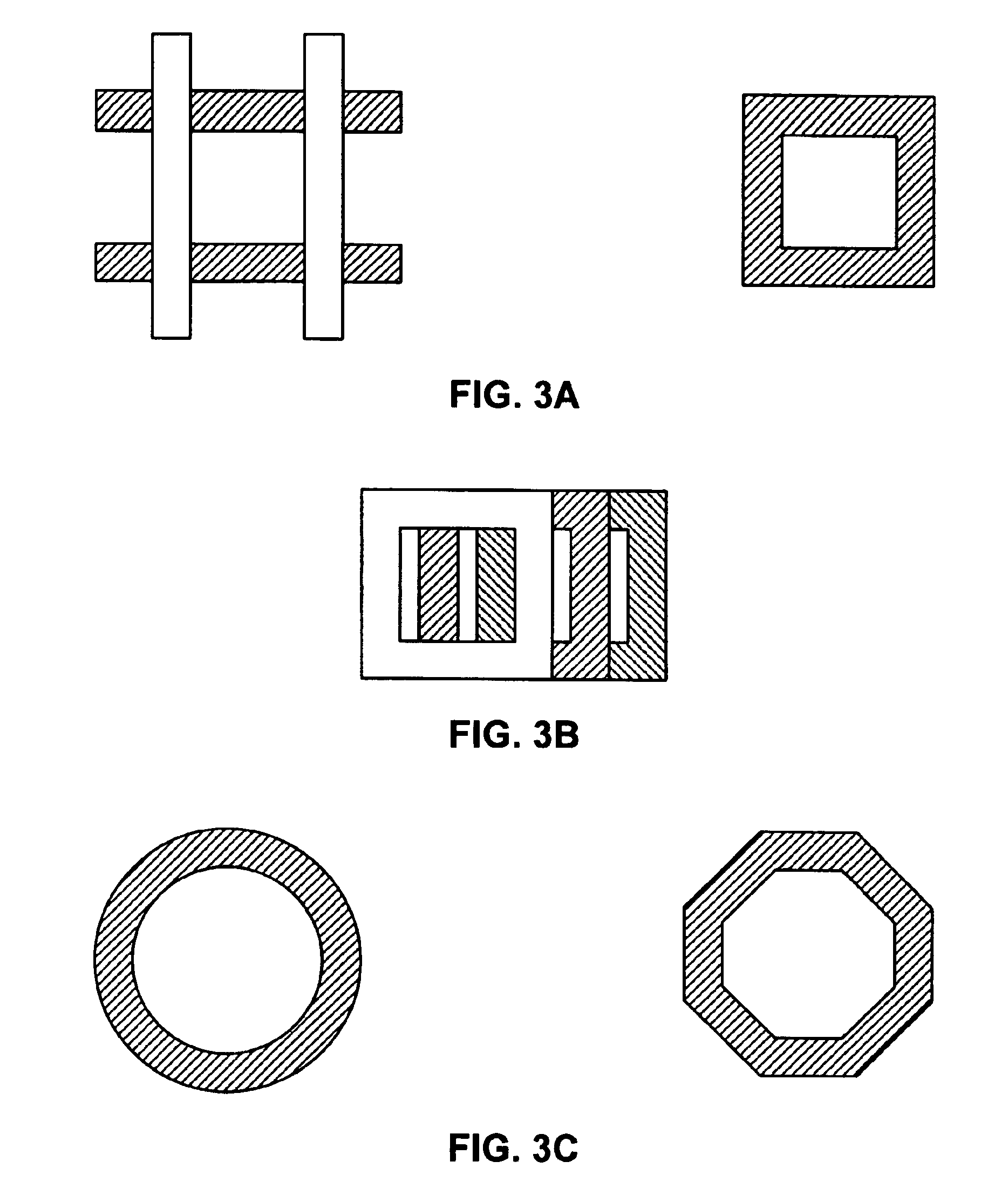
[0033]FIG. 1 illustrates two semiconductor dies in accordance with an embodiment of the present invention. One embodiment of the present invention provides a mechanism that aligns semiconductor die 102 to semiconductor die 104 to facilitate inter-chip communication between semiconductor die 102 and semiconductor die 104. As is...


PUM


Abstract

One embodiment of the present invention provides a system that facilitates aligning a first semiconductor die with a second semiconductor die, wherein the first semiconductor die and the second semiconductor die are arranged active face to active face. Note that the active face contains circuitry for communicating between semiconductor dies. The system starts by generating light on an active face of the first semiconductor die. The system then collimates the light within the active face of the first semiconductor die to form a first beam of light which is projected onto the second semiconductor die. Next, the system receives the first beam of light on an active face of the second semiconductor die and determines a position of the first beam of light on the active face of the second semiconductor die. Finally, the system determines an alignment of the second semiconductor die relative to the first semiconductor die based on the determined position of the first beam of light.

Description

RELATED APPLICATION[0001]This application hereby claims priority under 35 U.S.C. 119 to U.S. Provisional Patent Application No. 60 / 465,316, filed on 24 Apr. 2003, entitled, “A Light Emission Receiving Alignment Technique,” by inventors Robert J. Bosnyak and Robert J. Drost (Attorney Docket No. SUN-P9595PSP).GOVERNMENT LICENSE RIGHTS[0002]This invention was made with United States Government support under Contract No. NBCH020055 awarded by the Defense Advanced Research Projects Administration. The United States Government has certain rights in the invention.BACKGROUND[0003]1. Field of the Invention[0004]The present invention relates to integrated circuit devices. More specifically, the present invention relates to a method and an apparatus for optically aligning integrated circuit devices.[0005]2. Related Art[0006]Advances in semiconductor technology presently make it possible to integrate large-scale systems, including tens of millions of transistors, into a single semiconductor chi...

Claims


Application Information

Patent Timeline
Patent Type & Authority Patents(United States)
IPC IPC(8): H01L21/70H01L21/98H01L21/60H01L23/544
CPCH01L23/544H01L24/81H01L25/50H01L2223/54473H01L2223/5448H01L2224/16H01L2224/81121H01L2224/81801H01L2225/06527H01L2924/01013H01L2924/14H01L2924/01006H01L2924/01033H01L2924/01075H01L2924/12041H01L2924/12035H01L2924/12042H01L2924/12036H01L2924/00
Inventor BOSNYAK, ROBERT J.DROST, ROBERT J.
Owner ORACLE INT CORP
Why Eureka
Try Eureka