Memory device with quantum dot and method for manufacturing the same

a memory device and quantum dot technology, applied in the field of memory devices, can solve the problems of difficult to obtain junctions or quantum dots of this size, existing mosfets generate a large amount of heat, etc., and achieve the effect of high-effective and integrated memory devices

Inactive Publication Date: 2005-09-27
SAMSUNG ELECTRONICS CO LTD
View PDF15 Cites 50 Cited by
  • Summary
  • Abstract
  • Description
  • Claims
  • Application Information

AI Technical Summary

Benefits of technology

[0021]The present invention embodies a single electron device using the structure of a conventional semiconductor memory device. It is possible to control the size

Problems solved by technology

However, the existing MOSFET generates a large amount of heat.
If a lot of devices adapting the MOSFET are integrated in a small a

Method used


Image

  • Memory device with quantum dot and method for manufacturing the same
  • Memory device with quantum dot and method for manufacturing the same
  • Memory device with quantum dot and method for manufacturing the same

Examples


Embodiment Construction

[0028]The present invention will now be described more fully with reference to the accompanying drawings, in which a memory device according to preferred embodiments of the invention are shown and a method for manufacturing the same.

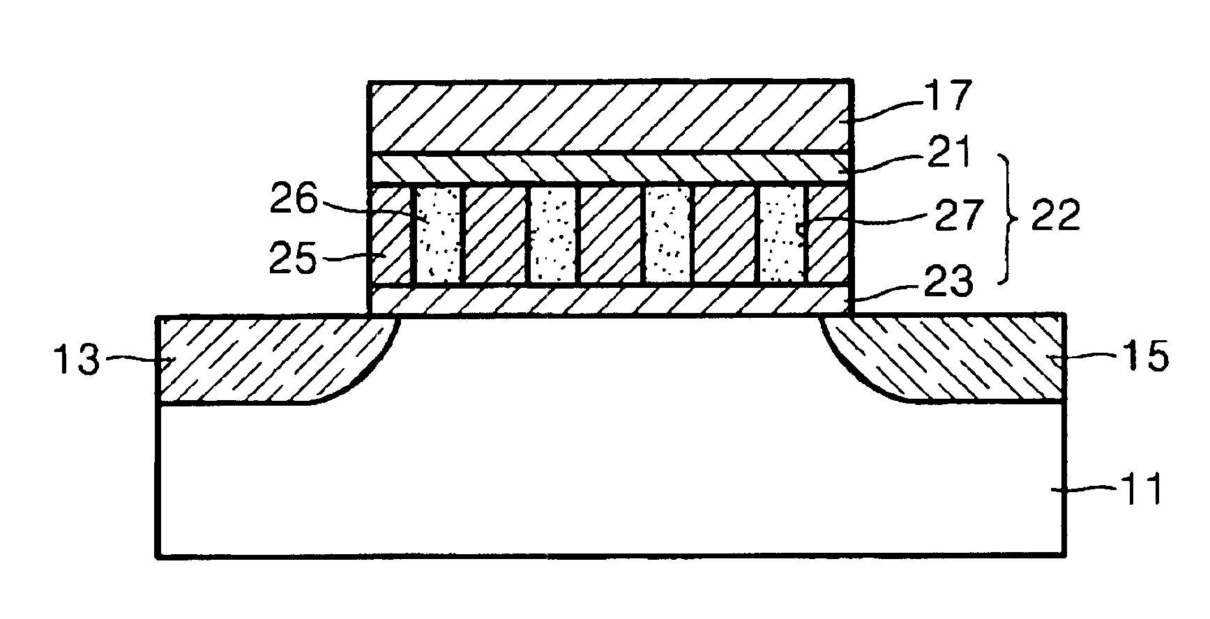
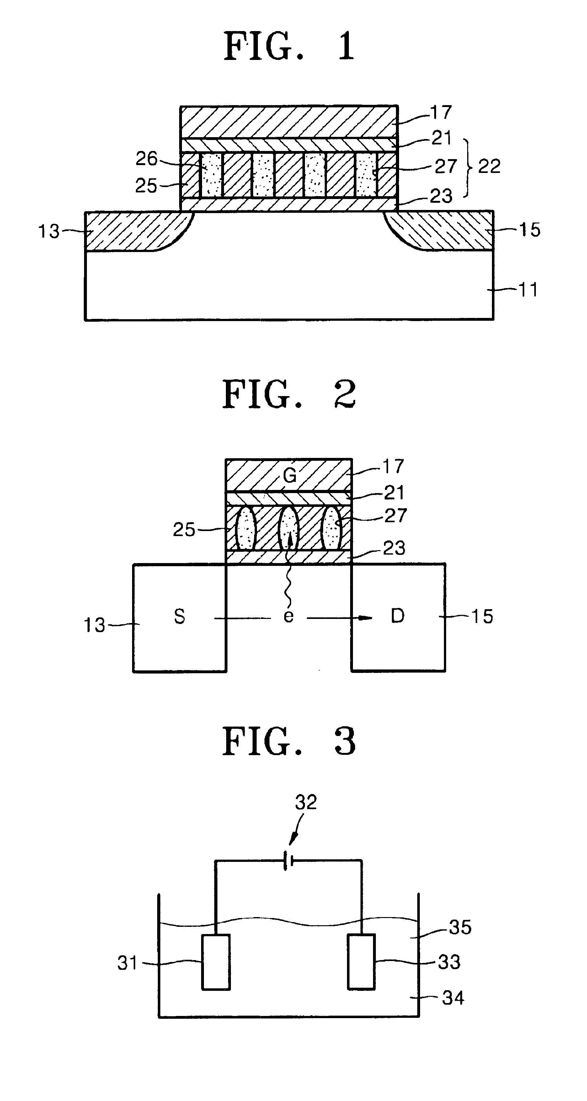
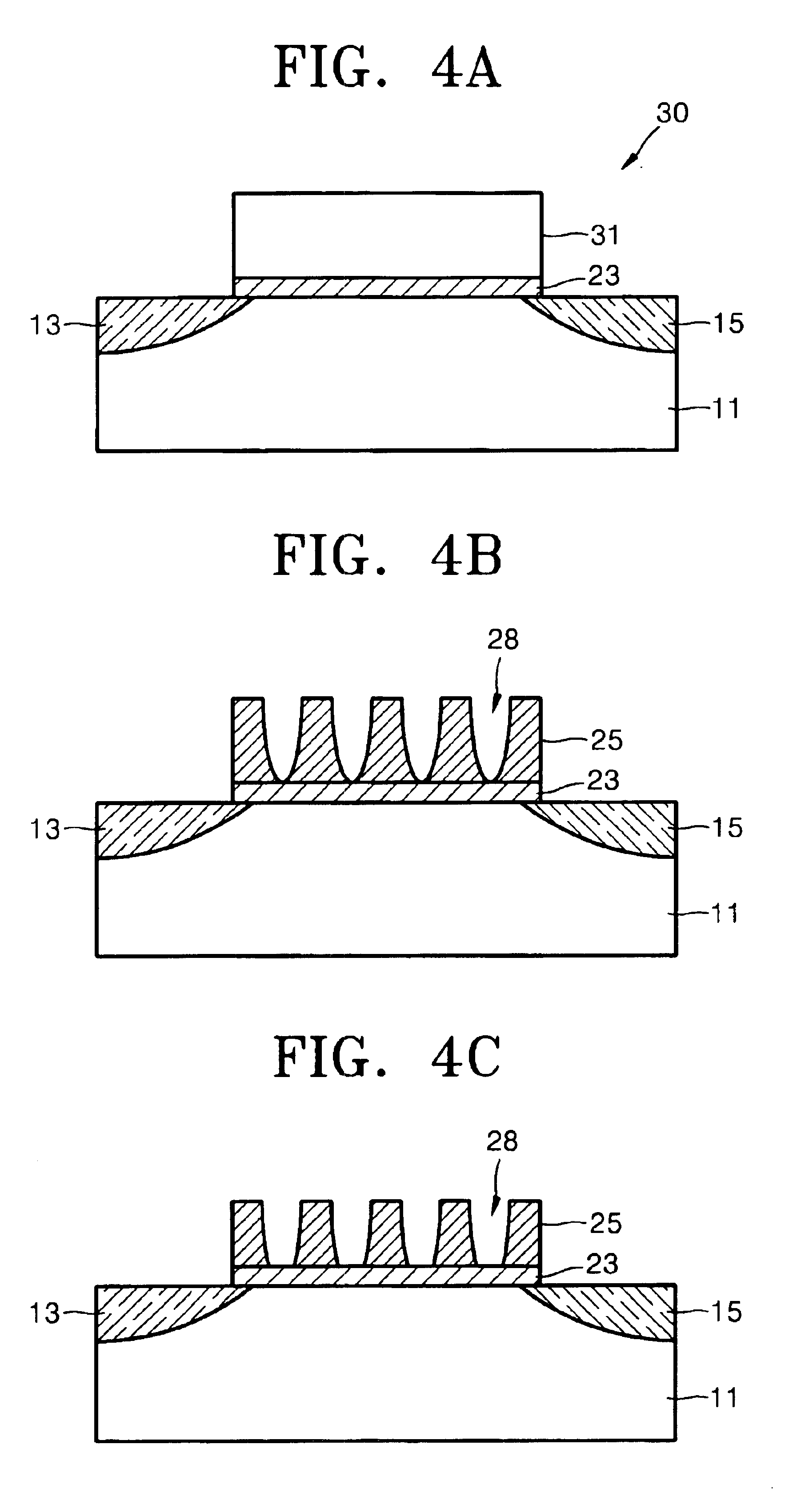
[0029]FIG. 1 is a view showing a memory device having a quantum dot according to an embodiment of the present invention. Referring to FIG. 1, the memory device having a quantum dot according to the embodiments of the present invention comprises a substrate 11; a source region 13 and a drain region 15 formed in the substrate so as to be separated from each other by a predetermined interval; a memory cell 22 which is formed on the surface of the substrate 11 to connect the source region 13 and the drain region 15, and has a plurality of nano-sized quantum dots 27 filled with material for storing electrons; and a control gate 17 which is formed on the memory cell 22 and controls the number of electrons stored in the memory cell 22.

[0030]The substrate 11 is ...


PUM


Abstract

Provided is a memory device formed using quantum devices and a method for manufacturing the same. A memory device comprises a substrate; a source region and a drain region formed in the substrate so as to be separated from each other by a predetermined interval; a memory cell which is formed on the surface of the substrate to connect the source region and the drain region, and has a plurality of nano-sized quantum dots filled with material for storing electrons; and a control gate which is formed on the memory cell and controls the number of electrons stored in the memory cell. It is possible to embody a highly efficient and highly integrated memory device by providing a memory device having nano-sized quantum dots and a method for manufacturing the same.

Description

[0001]Priority is claimed to Patent Application Number 2002-7708 filed in Republic of Korea on Feb. 9, 2002, herein incorporated by reference.BACKGROUND OF THE INVENTION[0002]1. Field of the Invention[0003]The present invention relates to a memory device and a method for manufacturing the same, and more particularly, to a memory device which is a single electron device and a method for manufacturing the same.[0004]2. Description of Related Art[0005]A semiconductor memory device includes two fundamental components: a transistor used as a switch for obtaining current paths, when writing or reading information onto or from a capacitor, and a capacitor for keeping the stored electric charges.[0006]It is necessary for a transistor to have a high transconductance (gm) characteristic so that a great deal of current flows in the transistor. Therefore, recent memory devices include Metal Oxide Semiconductor Field Effect Transistors (MOSFETS) adapted as switching devices, since they have a hi...

Claims


Application Information

Patent Timeline
IPC IPC(8): H01L21/28H01L21/02H01L29/40H01L29/66H01L29/423H01L29/788H01L29/06H01L21/8247H01L27/10H01L27/115H01L29/78H01L29/792
CPCB82Y10/00H01L21/28273H01L21/28282H01L29/42332H01L29/7881H01L29/7883Y10S977/943H01L29/40114H01L29/40117H01L29/78
Inventor CHOI, WON-BONGCHAE, SOO-DOO
Owner SAMSUNG ELECTRONICS CO LTD
Why Eureka
Try Eureka