Device having interdigital capacitor
- Summary
- Abstract
- Description
- Claims
- Application Information
AI Technical Summary
Benefits of technology
Problems solved by technology
Method used
Image

Examples
first embodiment
(First Embodiment)
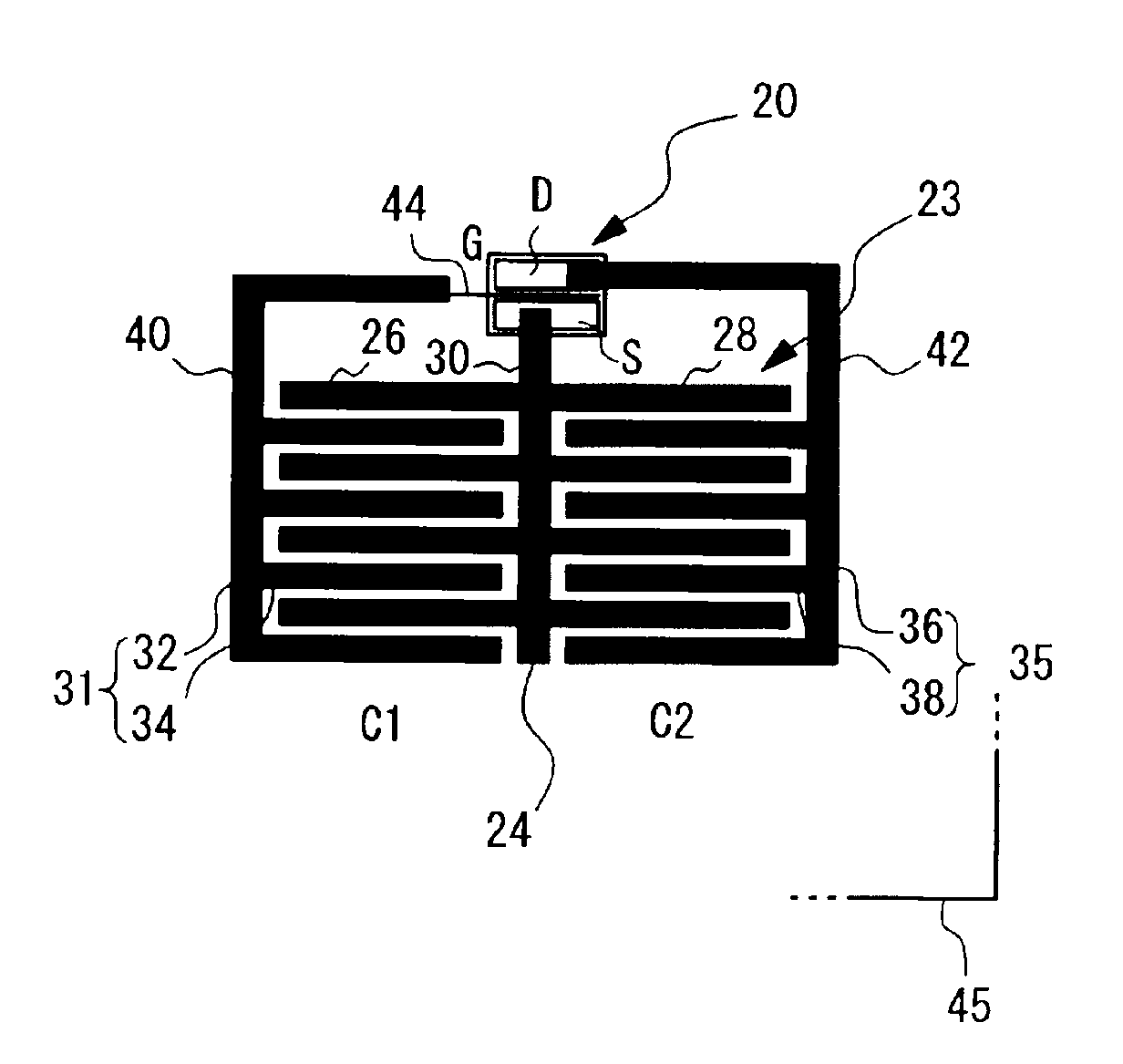
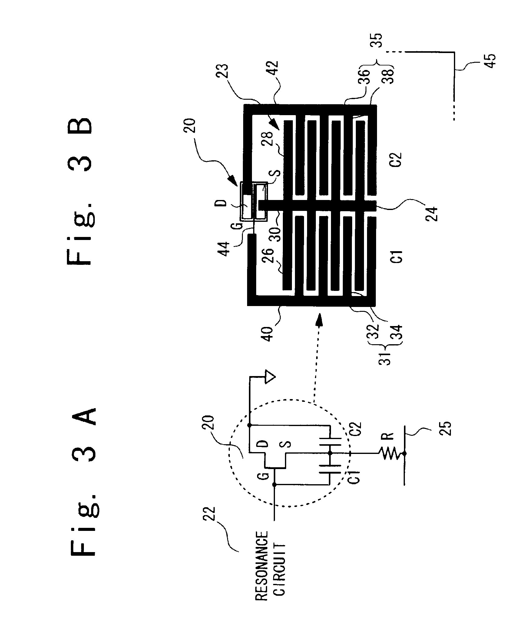
[0030]FIGS. 3A and 3B show a device according to a first embodiment of the present invention. More particularly, FIG. 3A is a circuit diagram of the device, and FIG. 3B is a plan view of a circuit pattern or layout of the device.
[0031]The device is an oscillator having a circuit configuration of FIG. 3A. The oscillator includes a field effect transistor 20, two capacitors C1 and C2, a bias resistor R and a resonance circuit 22. The capacitor C1 is connected between the gate G and source S of the transistor 20. The capacitor C2 is connected to the drain D and source S of the transistor 20. The drain D of the transistor 20 is held at a given potential (for example, the ground potential). The source S of the transistor 20 is connected to a power supply line 25 (via which a negative power supply voltage is available) via the bias resistor R. The resonance circuit 22 is connected to the gate G of the transistor 20. The capacitors C1 and C2 makes a capacitance division, ...
second embodiment
(Second Embodiment)
[0045]FIGS. 6A and 6B illustrate a device according to a second embodiment of the present invention. This device is a differential oscillator. FIG. 6A is a circuit diagram of the differential oscillator, and FIG. 6B shows a layout of a part surrounded by the broken line shown in FIG. 6A. In FIGS. 6A and 6B, parts that are the same as those shown in the previously described figures are given the same reference numerals.
[0046]Referring to FIG. 6A, the differential oscillator is composed of a first circuit part and a second circuit part. The first circuit part includes the transistor 20, the interdigital capacitors C1 and C2, a resonance circuit 56 and a bias resistor R1. The second circuit part includes a transistor 50, interdigital capacitors C3 and C4, a resonance circuit 58 and a bias resistor R2. Drains D of the transistors 20 and 50 are connected and set at a reference potential (for example, ground potential). The capacitors C2 and C3 are connected to a virtua...
third embodiment
(Third Embodiment)
[0050]FIG. 7 is a plan view of a device according to a third embodiment of the present invention. This device has a circuit pattern that realizes the circuit part surrounded by the broken line in FIG. 6A and differs from the circuit pattern shown in FIG. 6B. In FIG. 7, parts that are the same as those shown in the previously described figures are given the same reference numerals.
[0051]The device of FIG. 7 includes the transistors 20 and 50, the first and second interdigital capacitors C1 and C2 connected to the transistor 20, and the third and fourth interdigital capacitors C3 and C4 connected to the second transistor 50. The first and second interdigital capacitors C1 and C2 have the first common electrode 123 including the straight bus line 24. The third and fourth interdigital capacitors C3 and C4 have a second common electrode 523, which includes a straight bus line 524. The bus line 24 of the first common electrode 123 is aligned with the bus line 524 of the ...
PUM
 Abstract
Description
Claims
Application Information
 - R&D Engineer
- R&D Manager
- IP Professional
- Industry Leading Data Capabilities
- Powerful AI technology
- Patent DNA Extraction
Browse by: Latest US Patents, China's latest patents, Technical Efficacy Thesaurus, Application Domain, Technology Topic.
© 2024 PatSnap. All rights reserved.Legal|Privacy policy|Modern Slavery Act Transparency Statement|Sitemap