Low parasitic inductance power module and double-faced heat-dissipation low parasitic inductance power module
Active Publication Date: 2021-05-20
YANGZHOU GUOYANG ELECTRONICS CO LTD
View PDF0 Cites 2 Cited by
Summary
Abstract
Description
Claims
Application Information
AI Technical Summary
This helps you quickly interpret patents by identifying the three key elements:
Problems solved by technology
Method used
Benefits of technology
Benefits of technology
The present invention provides a power module with low parasitic inductance and small size. The module has a double-sided heat-dissipation design for improved thermal efficiency. By arranging the chips and electrodes on the faces of both metal insulating substrates, a loop parasitic inductance is reduced, leading to a smaller size, lower cost, and improved reliability of the module. Additionally, heat sinks can be added on both sides of the module for further heat dissipation efficiency. Overall, this innovation simplifies the structure of the module and improves its thermal performance.
Problems solved by technology
The present power module in power electronics has a large package volume and a heavy weight, which does not meet the requirements of high power density and light weight in the fields of electromobiles, aerospace and the like.
The power module in power electronics with a larger volume often has a larger parasitic inductance, which will result in a larger overshoot voltage and increase losses, and also limit the application of the power module in a high switching frequency occasion.
A SiC power electronic device has the characteristics of high frequency, high temperature and high efficiency, but the present power module has a larger parasitic inductance, which limits the performance implementation of the SiC.
In addition, with the continuous upgrading of the power density at an application end, a package structure of the present power module has hindered the further improvement of the power density, and a more effective heat dissipation structure has to be developed to meet the increasing demand of the power density.
In addition, a power terminal and a control terminal are only connected with a first lining plate, so that the arrangement is not flexible enough, an area of the lining plate cannot be further reduced, and losses are increased due to a long current path.
Method used
Image
Click on the blue label to locate the original text in one second.
Reading with bidirectional positioning of images and text.
Examples
embodiment 1
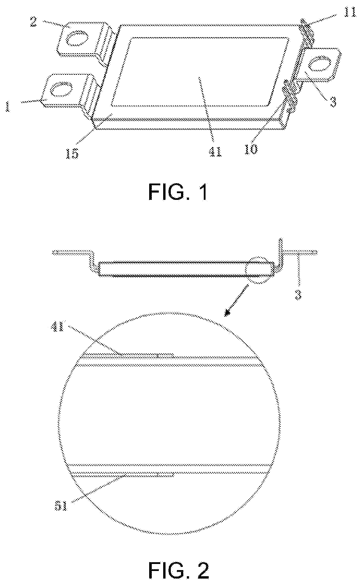
[0063]According to the invention, a switch chip and a freewheeldiodechip of a relative bridge arm are stacked, so that a commutating loop path is shortest, thereby greatly reducing a parasitic inductance of the loop. The purpose of double-faced heat dissipation is achieved by arranging heat dissipation paths on both sides of the stacked chips, thus further reducing a thermal resistance of a power module.
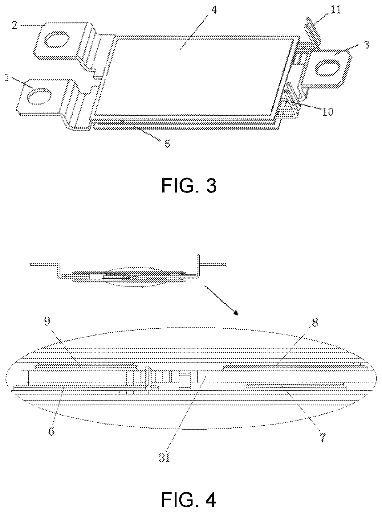
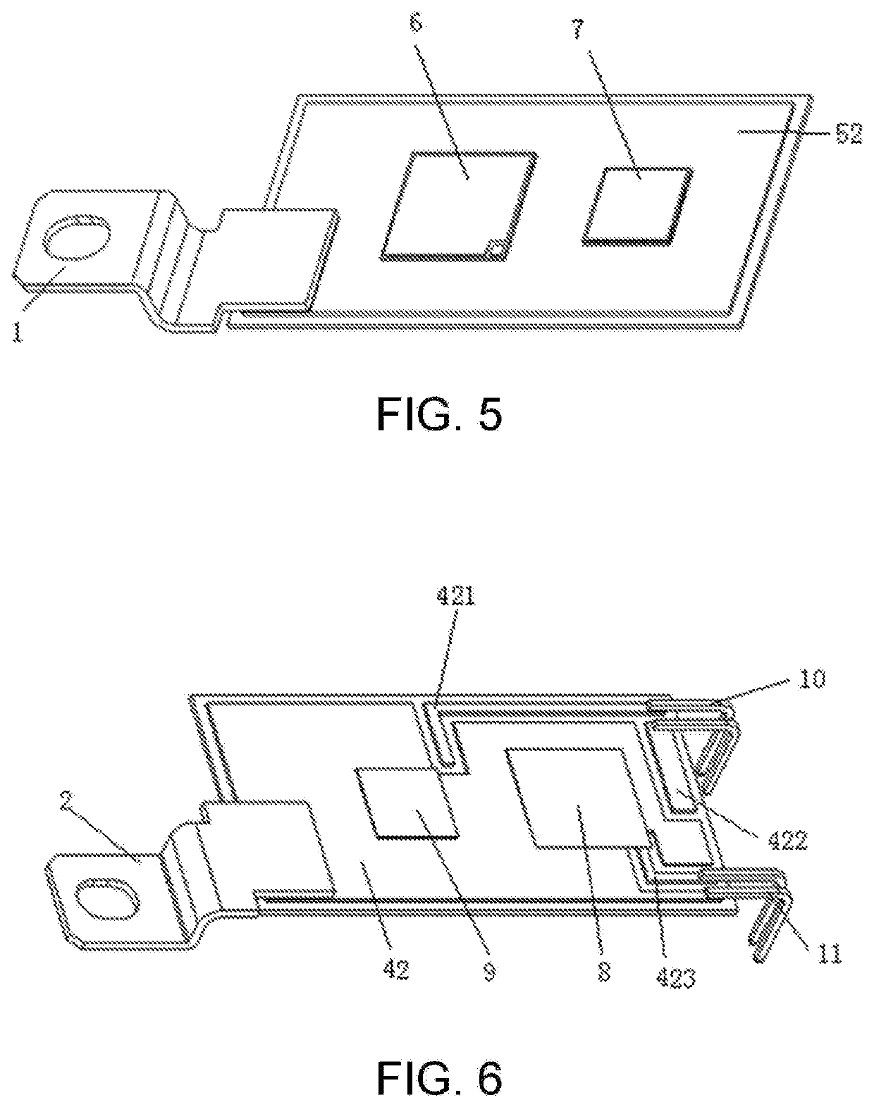
[0064]As shown in FIG. 1, a double-faced heat-dissipation low parasitic inductance power module includes a positive power terminal 1, a negative power terminal 2, an output power terminal 3, a bottom metal insulating substrate 5 connected with the positive power terminal 1, a top metal insulating substrate 4 connected with the negative power terminal 2, an upper half-bridge driving terminal 10, a lower half-bridge driving terminal 11 and a plastic package shell 15 used for encapsulating. The positive power terminal 1 in the embodiment is sintered on the bottom metal insulating subs...
embodiment 2
[0074]As shown in FIG. 14, the structure of this embodiment is basically the same as that of Embodiment 1, but differs in that the welding portion of the output power terminal 3 in the embodiment is a matrix 311 at a position contacted with the chip, and is a three-layer structure at a position not contacted with the chip, the matrix 311 is located in a middle layer, and fillers 312 are located at upper and lower sides. The matrix 311 is metal molybdenum or tungstencopper with small thermal expansion coefficients, and the filler 312 is metal silver with good conductivity.
[0075]In this embodiment, the power chip is sintered on the molybdenum matrix 311 of the output electrode, and a groove is machined in a part of the output electrode that is not contacted with the chip, and the groove is filled with silver. The thermal expansion coefficient of the metal molybdenum is generally one third of that of copper, which is close to that of the chip. During the operation of the power module,...
embodiment 3
[0076]As shown in FIG. 15, the structure of this embodiment is basically the same as that of Embodiment 1, but differs in that a stress buffer layer 14 is filled between the welding portion 31 of the output power terminal 3 and the chip, the welding portion 31 of the output power terminal 3 is metallic copper, and the stress buffer layer 14 is metallic molybdenum or tungsten copper.
[0077]The output electrode is made of pure copper. Due to a larger difference in thermal expansion between the copper and the chip, in order to improve the long-term reliability of the pad layer 16, the stress buffer layer 14 is added between the chip and the output electrode for transition in this embodiment, i.e., metal molybdenum or tungsten copper is sintered on the surface of the chip, and then molybdenum or tungsten copper is sintered on the output electrode.
PUM
Abstract
A low parasitic inductancepower module, which includes an input power terminal, an output power terminal, a top metal insulating substrate, a bottom metal insulating substrate and a plastic package shell, wherein the input power terminal includes a positive power terminal and a negative power terminal, the top metal insulating substrate and the bottom metal insulating substrate are stacked, chips are sintered on faces of both the top metal insulating substrate and the bottom metal insulating substrate opposite to each other, and the positive power terminal, the negative power terminal, and the output power terminal are all electrically connected with the chips; and the output power terminal includes a welding portion and a connecting portion located outside the plastic package shell, and the welding portion is located between the top metal insulating substrate and the bottom metal insulating substrate.
Description
BACKGROUNDTechnical Field[0001]The present invention relates to a power module in power electronics, and more particularly, to a low parasitic inductancepower module and a double-faced heat-dissipation low parasitic inductance power module.Description of Related Art[0002]A power electronics technology plays a very important role in the rapidly developed industrial field today. As a representative of the power electronics technology, a power module in power electronics has been widely used in electromobiles, photovoltaic power generation, wind power generation, industrial frequency conversion and other industries. With the rise of industry of China, the power module in power electronics has a broader market prospect.[0003]The present power module in power electronics has a large package volume and a heavy weight, which does not meet the requirements of high power density and light weight in the fields of electromobiles, aerospace and the like. The power module in power electronics w...
Claims
Application Information
Patent Timeline
Application Date:The date an application was filed.
Publication Date:The date a patent or application was officially published.
First Publication Date:The earliest publication date of a patent with the same application number.
Issue Date:Publication date of the patent grant document.
PCT Entry Date:The Entry date of PCT National Phase.
Estimated Expiry Date:The statutory expiry date of a patent right according to the Patent Law, and it is the longest term of protection that the patent right can achieve without the termination of the patent right due to other reasons(Term extension factor has been taken into account ).
Invalid Date:Actual expiry date is based on effective date or publication date of legal transaction data of invalid patent.

