Silicon oxycarbide, growth method of silicon oxycarbide layer, semiconductor device and manufacture method for semiconductor device

a technology of silicon oxycarbide and growth method, which is applied in the direction of chemical vapor deposition coating, basic electric elements, coatings, etc., can solve the problems of difficult to use wiring materials having a resistivity lower than cu, narrow wiring space, and inability to improve the overall operation speed. , to achieve the effect of preventing peeling and cracking

Active Publication Date: 2005-09-27
FUJITSU LTD
View PDF5 Cites 45 Cited by
  • Summary
  • Abstract
  • Description
  • Claims
  • Application Information

AI Technical Summary

Benefits of technology

The technical effect of this patent is to prevent peeling and cracks in the insulating layers of multi-layer wirings.

Problems solved by technology

The technical problem addressed in this patent text is the need to reduce parasitic capacitance in multi-layer wiring structures of semiconductor integrated circuit devices, which can impact device operation speed. This is achieved by using low dielectric constant insulating layers with low adhesion to the underlying layer, but this can lead to film peel-off at the interface and cracks in the insulating layer with the low relative dielectric factor. The patent proposes a solution using a lamination of multiple low dielectric constant insulating layers with different thermal expansion coefficients to reduce stress and prevent cracks.

Method used


Image

  • Silicon oxycarbide, growth method of silicon oxycarbide layer, semiconductor device and manufacture method for semiconductor device
  • Silicon oxycarbide, growth method of silicon oxycarbide layer, semiconductor device and manufacture method for semiconductor device
  • Silicon oxycarbide, growth method of silicon oxycarbide layer, semiconductor device and manufacture method for semiconductor device

Examples


Embodiment Construction

[0042]With reference to the accompanying drawings, description will be made on the experiments made by the present inventors and the results thereof and on the embodiments of the invention.

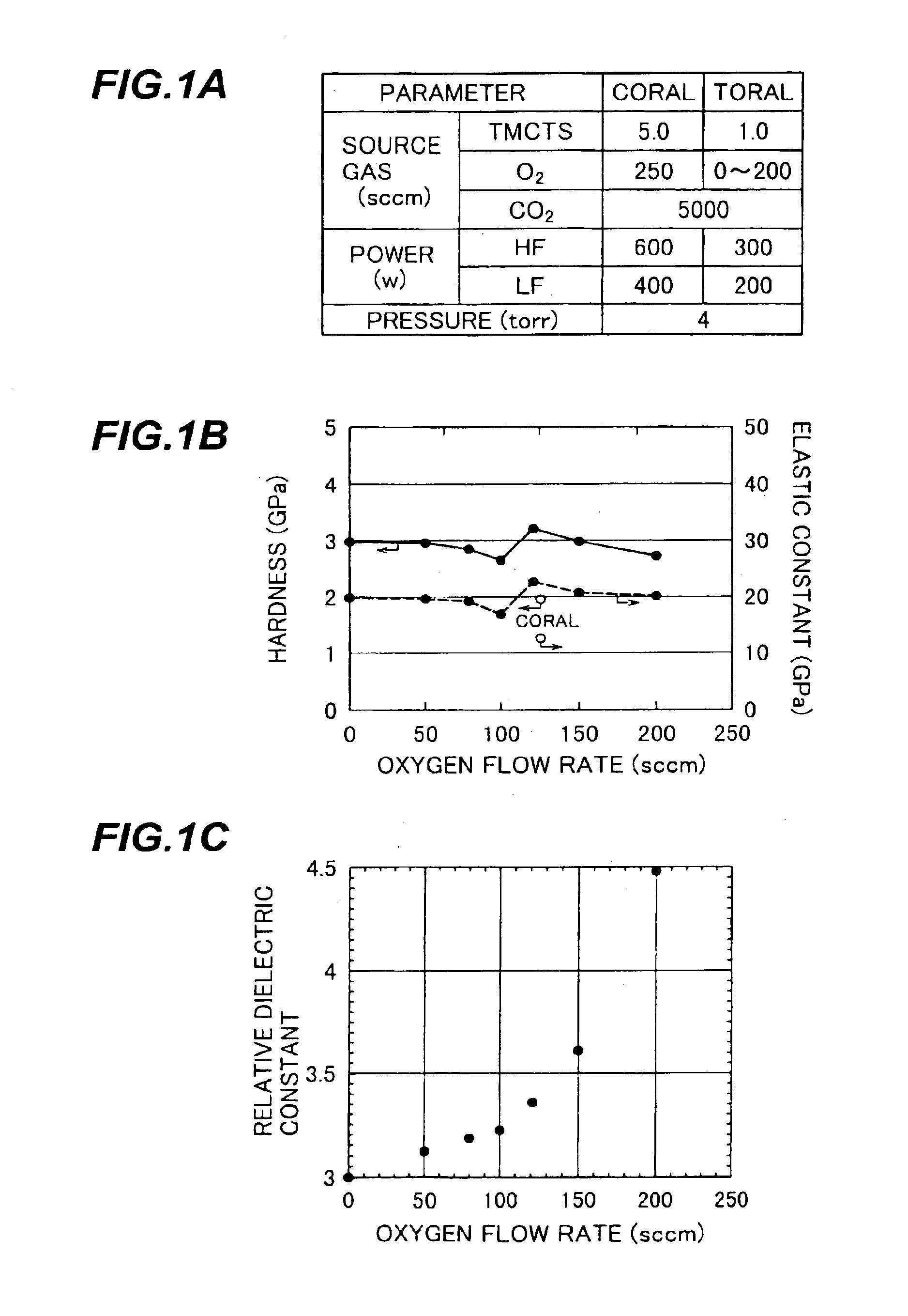
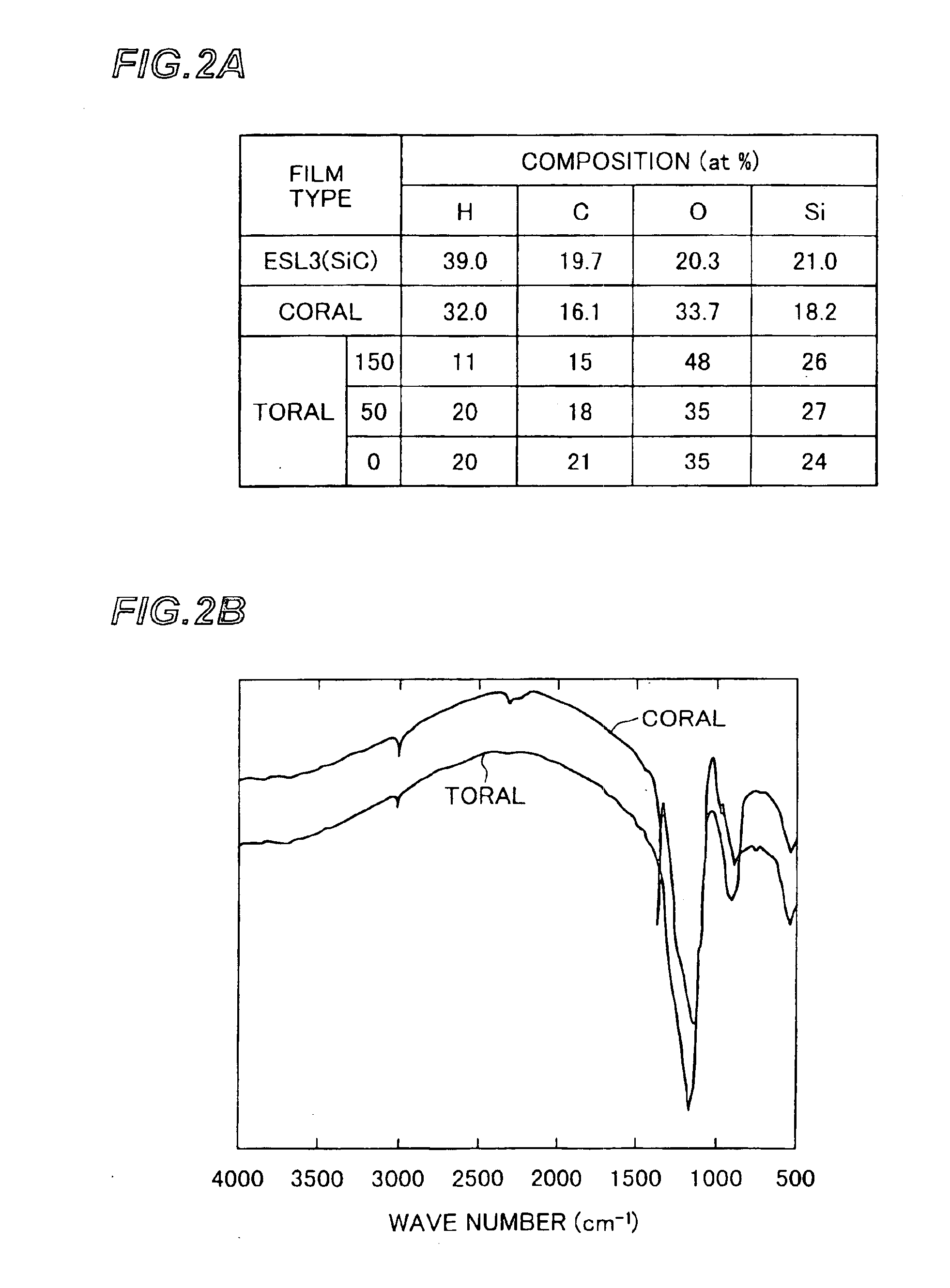
[0043]A vapor-grown silicon oxycarbide (registered trademark CORAL) film available from Novellus Systems, Inc., has a low relative dielectric factor of about 2.9. However, it has weak adhesion to an SiC layer or the like and is rather insufficient in terms of the physical strength such as hardness and elastic constant or Young's modulus.

[0044]The present inventors have developed new CVD conditions to improve tight adhesion of a vapor-grown silicon oxycarbide film and increase the physical strength. In the following, a conventional vapor-grown silicon oxycarbide film is called CORAL, and a vapor-grown silicon oxycarbide film developed by the present inventors is called TORAL or new SiOC. TORAL or new SiOC is considered having Si—O—C as its main skeleton.

[0045]FIG. 1A is a table showing growth param...


PUM

PropertyMeasurementUnit
Fractionaaaaaaaaaa
Fractionaaaaaaaaaa
Pressureaaaaaaaaaa

Abstract

A semiconductor device including an underlying structure having a silicon carbide layer covering a copper wiring, and growing silicon oxycarbide on the underlying structure by vapor deposition using, as source gas, tetramethylcyclotetrasiloxane, carbon dioxide gas and oxygen gas, a flow rate of said oxygen gas being at most 3% of a flow rate of the carbon dioxide gas. The surface of the silicon carbide layer of the underlying structure may be treated with a plasma of weak oxidizing gas which contains oxygen and has a molecular weight larger than that of O2 to bring the surface more hydrophilic. Film peel-off and cracks in the interlayer insulating layer decrease.

Description


Claims


Application Information

Patent Timeline
Owner FUJITSU LTD
Why Eureka
Try Eureka