Electrode portion structure

a technology of electrode portion and electrode, which is applied in the direction of basic electric elements, printed circuit manufacturing, solid-state devices, etc., can solve the problems of generating the disconnection between the electrode and the end face of the through-electrode b>15/b>, and is difficult to achieve, so as to reduce the resistance of the connection portion, improve the high-volume production property, and prevent the effect of generating the disconnection

Inactive Publication Date: 2011-09-15
ORMON CORP
View PDF16 Cites 6 Cited by
  • Summary
  • Abstract
  • Description
  • Claims
  • Application Information

AI Technical Summary

Benefits of technology

[0022]In the electrode portion structure according to another aspect of the invention, the end face of the through-electrode is formed by a curved surface. Accordingly, because the end face of the through-electrode can be formed into the curved surface, the end face of the through-electrode can be adjusted by polishing the substrate, thereby improving the high-volume production property.
[0023]In the electrode portion structure according to still another aspect of the invention, the whole end face of the through-electrode is exposed from the opening of the insulating film. Accordingly, a connection area between the end face of the through-electrode and the electrode can be maximized to reduce a resistance of a connection portion between the through-electrode and the electrode.
[0024]In the electrode portion structure according to an aspect of the invention, the opening of the insulating film is formed inside an outer circumference of the through-electrode. Accordingly, the exposure of the substrate from the insulating film due to the variation in making the contact hole can be prevented, and the required accuracy can be loosened in making the contact hole. Additionally, because an upper limit of the projection length Dtsv of the through-electrode can be increased, an allowable range or an adjustable range of the projection length Dtsv of the through-electrode is widened to facilitate the design and production of the electrode portion.

Problems solved by technology

However, from the technical viewpoint, it is actually difficult that a step between the end face of the through-electrode 15 and the surface of the substrate 12 is decreased to the order or less of sub-micrometer to flatten the end face of the through-electrode 15 flush with the surface of the substrate 12.
Therefore, when thermal expansion and contraction are generated by a temperature change, an internal stress generated between the joining material 21 and the circuit substrate 22 or the electrode 13 is increased to easily generate peel-off or a crack in the joined portion, which results in a risk of generating the disconnection between the electrode 13 and the circuit substrate 22.
When flatness of the substrate and through-electrode is obtained by the method of Japanese Unexamined Patent Publication No. 7-283536, the polishing condition changes depending on the material, the shape, and dimensions of the through-electrode, and time and cost are increased to determine the optimum polishing condition through a trial and error process, and development time is lengthened while the cost for the electrode structure is increased.

Method used


Image

  • Electrode portion structure
  • Electrode portion structure
  • Electrode portion structure

Examples


Embodiment Construction

[0049]Hereinafter, embodiments of the present invention will be described with reference to the drawings. In embodiments of the invention, numerous specific details are set forth in order to provide a more thorough understanding of the invention. However, it will be apparent to one of ordinary skill in the art that the invention may be practiced without these specific details. In other instances, well-known features have not been described in detail to avoid obscuring the invention. Additionally, the invention is not limited to the following embodiments, but various design changes can be made without departing from the scope of the invention.

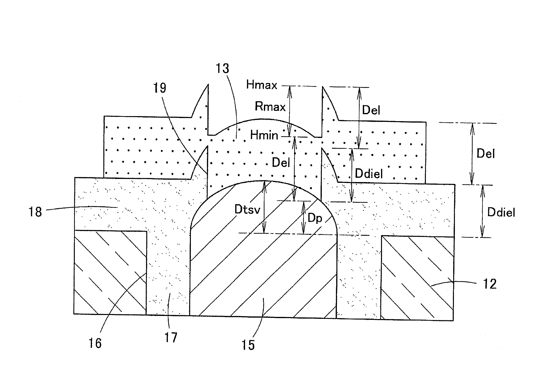
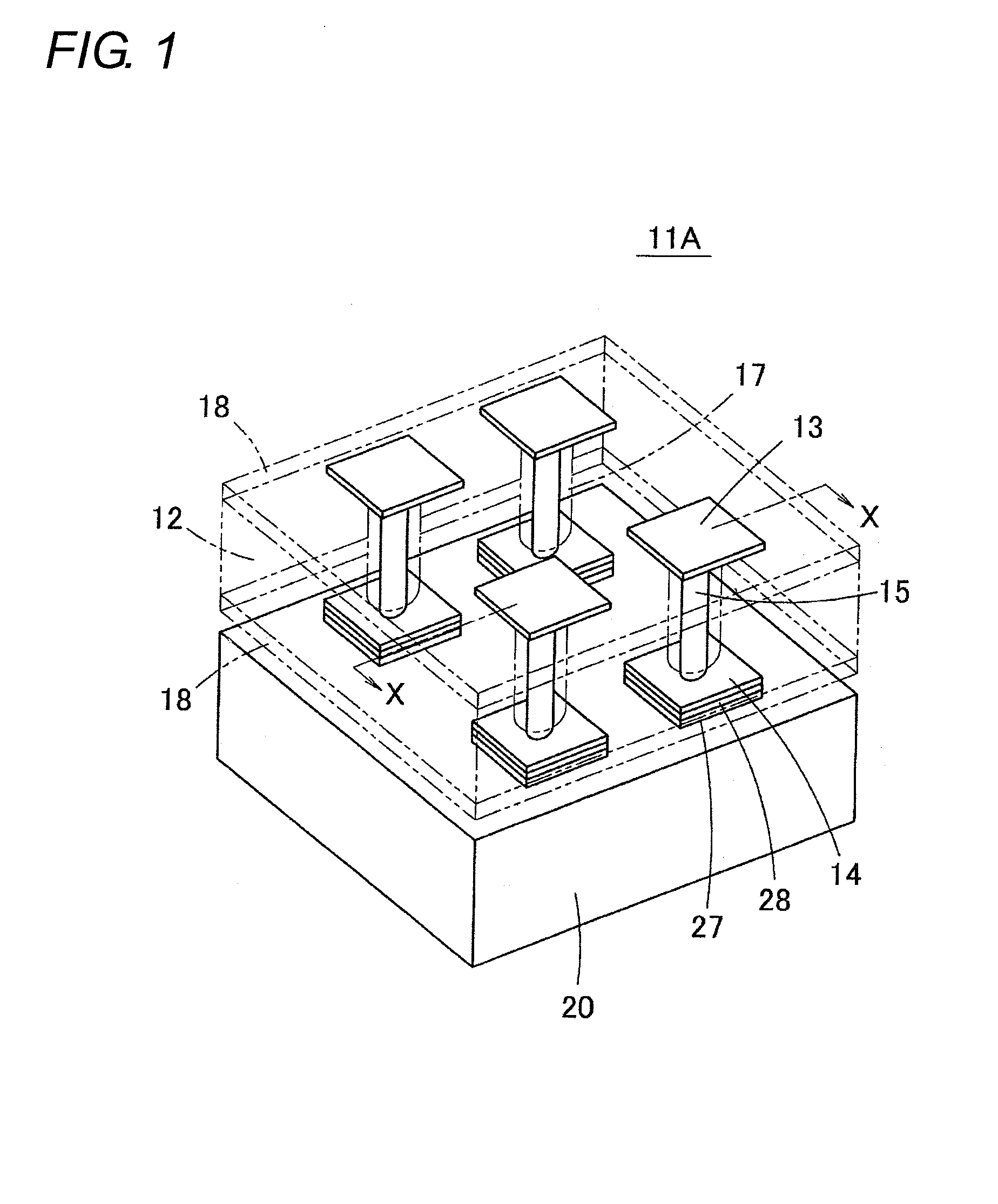
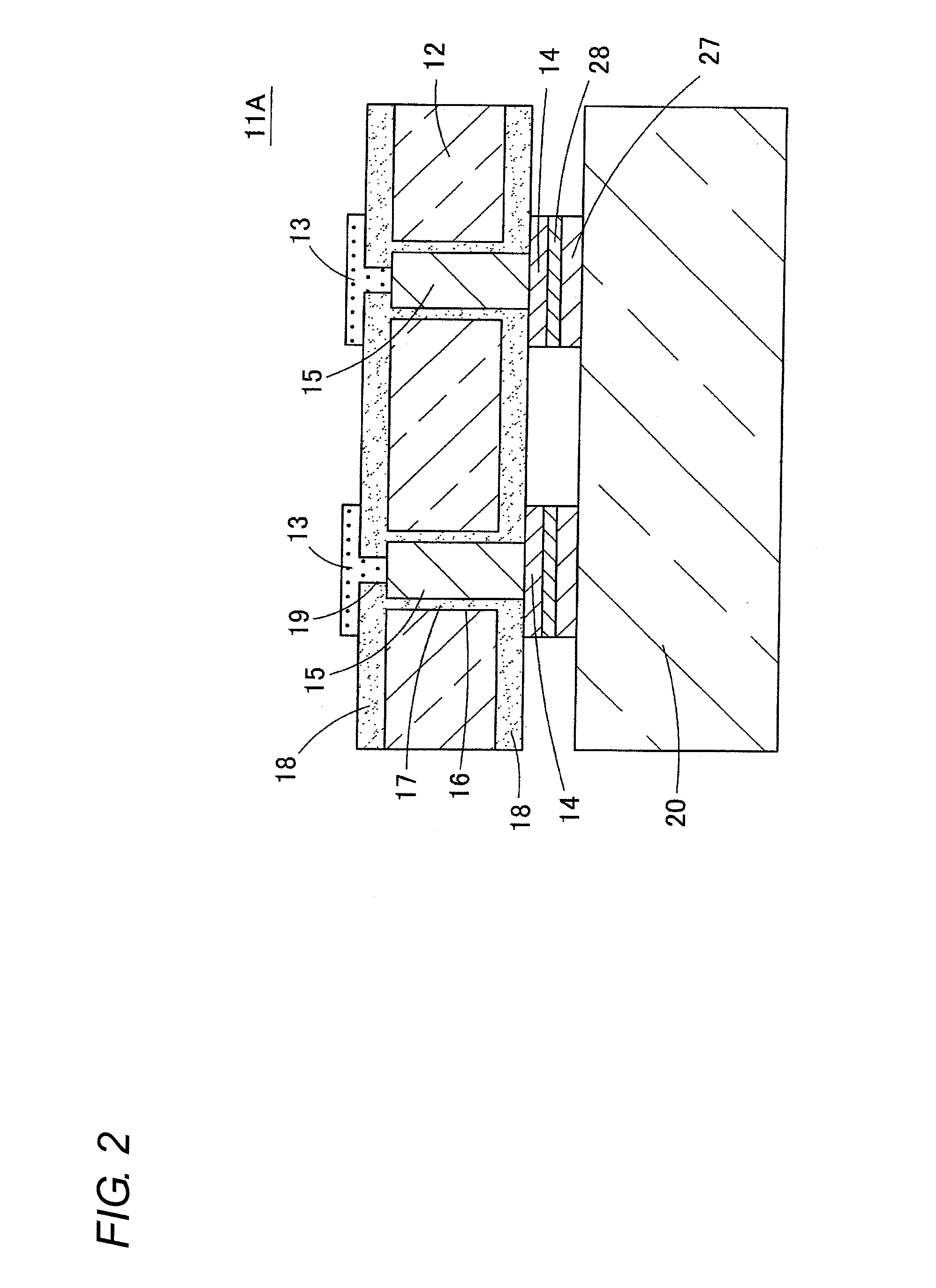
[0050]FIG. 10 is an enlarged sectional view illustrating an electrode portion structure according to an embodiment of the invention. For example, the electrode portion structure is used in an electrode structure 11A illustrated in FIGS. 1 and 2 and an electrode structure 11B illustrated in FIG. 4. In the electrode portion structure of an embodim...


PUM


Abstract

In an electrode portion structure in which an electrode is formed in an end portion of a through-wiring, disconnection is prevented in an electrode portion. A through-hole that vertically pierces a substrate is made in the substrate, and a through-electrode is provided in the through-hole. The through-electrode is projected in s curved-surface manner from an upper surface of the substrate. The upper surface of the substrate 12 is coated with an insulating film, and a contact hole is made in the insulating film while aligned with the through-electrode. An opening diameter of the contact hole is lower than a sectional diameter of the through-electrode, and surroundings of an upper surface of the through-electrode are coated with the contact hole. A thickness Ddiel of the insulating film is equal to or lower than a projection length Dp of the through-electrode from the upper surface of the substrate at an opening edge of the contact hole. Additionally, assuming that Dtsv is a projection length (maximum projection length) of an apex of the through-electrode from the upper surface of the substrate, the projection length Dtsv is adjusted so as to become 0≦Dtsv≦Ddiel+Dp (Dp>0).

Description

BACKGROUND OF THE INVENTION[0001]1. Technical Field[0002]The present invention relates to an electrode portion structure, specifically to an electrode portion structure in which an electrode is formed in an end portion of through-wiring.[0003]2. Related Art[0004]FIGS. 1 and 2 are a schematic perspective view and a sectional view illustrating an example of an electrode structure in which the electrode is formed in the end portion of the through-wiring, respectively. In an electrode structure 11A, an electrode 13 is formed in an upper surface of a substrate 12, an electrode 14 is formed in a lower surface of the substrate 12, and the electrodes 13 and 14 located in the upper surface and lower surface of the substrate 12 are electrically connected by a through-electrode 15 piercing the substrate 12.[0005]As illustrated in FIGS. 1 and 2, a through-hole 16 is made from the upper surface to the lower surface of the substrate 12, an inner circumferential surface of the through-hole 16 is c...

Claims


Application Information

Patent Timeline
Patent Type & Authority Applications(United States)
IPC IPC(8): H05K1/11H01L21/3205H01L21/768H01L23/522
CPCH05K3/4038H01L21/76898H01L2924/0002H01L2224/05554H01L2224/16145H01L2224/16238H01L2224/16146H01L2224/131H01L2224/05572H01L24/05H01L24/06H01L24/13H01L24/16H01L2224/0401H01L2224/05557H01L2224/05558H01L2224/0557H01L2224/05644H01L2224/05669H01L2224/06181H01L2224/05568H01L2924/00014H01L2924/014H01L2224/05552
Inventor DOI, SAYAKAOKUNO, TOSHIAKISANO, AKIHIKOMIYAJI, TAKAAKIHADA, YOSHIKI
Owner ORMON CORP
Why Eureka
Try Eureka