Embedded chip semiconductor having dual electronic connection faces

a semiconductor and chip technology, applied in the field of semiconductor packages, can solve the problems of limited production rate of semiconductor packages and limited semiconductors in one direction, and achieve the effect of increasing mass production

Inactive Publication Date: 2005-12-15
CHANG ROGER
View PDF28 Cites 18 Cited by
  • Summary
  • Abstract
  • Description
  • Claims
  • Application Information

AI Technical Summary

Benefits of technology

[0010] The main objective of the invention is to provide an embedded chip semiconductor package having dual electronic connection faces. The present invention is fabricated with a printed circuit board fabrication process to effectively increase the mass production and has different connection ways for connecting to an external circuit board or other electronic elements.

Problems solved by technology

Therefore, the production rate of the semiconductor packages is limited by the conventional production process.
Therefore, the semiconductor is limited to one way of connecting to the external circuit board.

Method used


Image

  • Embedded chip semiconductor having dual electronic connection faces
  • Embedded chip semiconductor having dual electronic connection faces
  • Embedded chip semiconductor having dual electronic connection faces

Examples


Embodiment Construction

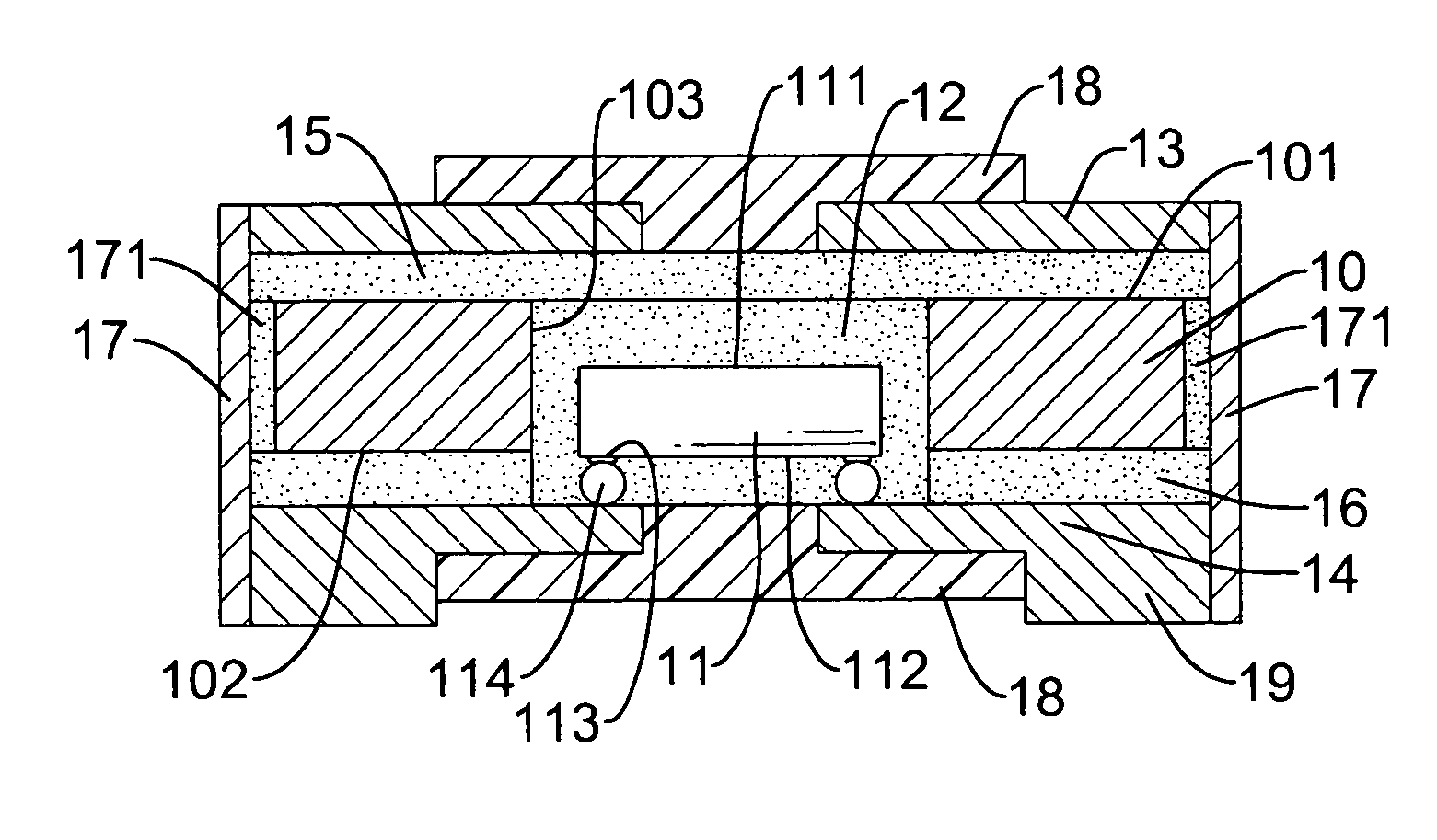
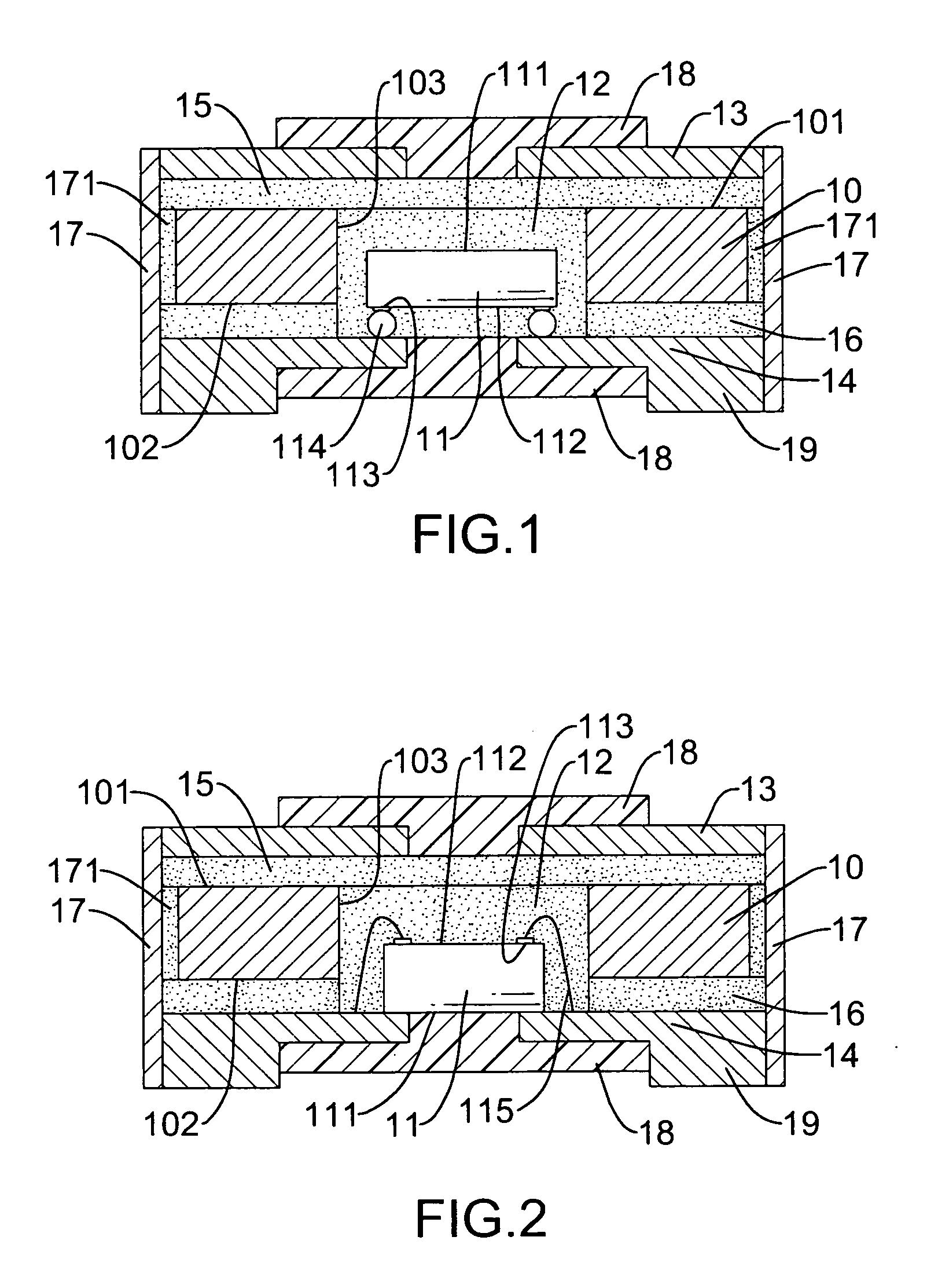
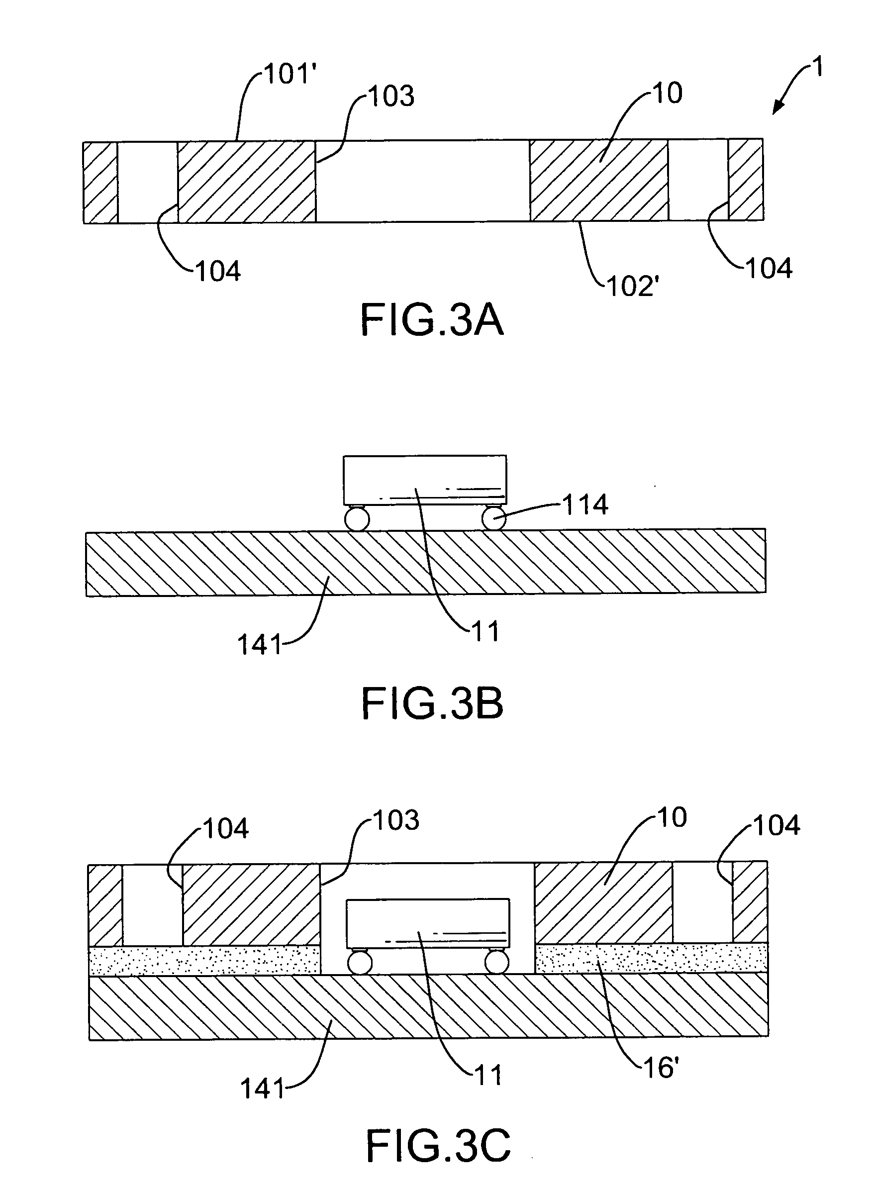
[0017] An embedded chip semiconductor in accordance with the present invention is fabricated with a printed circuit board fabrication process so the single embedded chip semiconductors can be mass-produced and has dual electronic connection faces.

[0018] With reference to FIG. 1, a first embodiment of an embedded chip semiconductor in accordance with the present invention includes a substrate (10), at least one chip (11), an encapsulant (12), a first insulation layer (15), a second insulation layer (16), a first circuit pattern (13), a second circuit pattern (14), multiple conduct vias (17), multiple separations (171) and two optional protective layers (18).

[0019] The substrate (10) has a thickness (not numbered), a top surface (101), a bottom surface (102) and at least one chip recess (103). In the first embodiment, the substrate (10) is metallic. The substrate (10) is able to be nonmetallic.

[0020] Each chip (11) has a thickness (not numbered), a top face (111), a bottom face (11...


PUM


Abstract

An embedded chip semiconductor has a substrate, at least one chip, an encapsulant, two circuit patterns and multiple contact vias. The substrate has a top surface, a bottom surface and at least one chip recess. The at least one chip has multiple terminals and is mounted in a corresponding chip recess. The thickness of the chip is equal to or less than the thickness of the substrate. The encapsulant is formed in the chip recess to hold the chip. The circuit patterns are respectively formed on the top and bottom surfaces of the substrate and one of the circuit patterns is connected to the multiple terminals of the chip. The two circuit patterns on two surfaces of the substrate are connected through the multiple contact vias. Therefore, the semiconductor has dual electronic connection faces to be suitable for different applications.

Description

BACKGROUND OF THE INVENTION [0001] 1. Field of the Invention [0002] The present invention relates to a semiconductor package and more particularly to an embedded chip semiconductor fabricated with a printed circuit board fabrication process to form dual electronic connection faces. [0003] 2. Description of Related Art [0004] With reference to FIG. 4, a conventional semiconductor package (50) comprises a leadframe (500), a chip (60) having I / O terminals (601), molded encapsulant (80) and wire bondings (70). The leadframe has a die pad (52) and multiple leads (51) around the die pad (52). A general process to package the semiconductor package (50) includes the following steps: [0005] (a) mounting the chip (60) on the die pad (52) of the leadframe (500); [0006] (b) connecting the I / O terminals (601) of the chip (60) to the leads (51) of the leadframe (500) by the wire bondings (70); and [0007] (c) encapsulating the chip (60), wire bondings (70) and portions of the leadframe (500) with ...

Claims


Application Information

Patent Timeline
Patent Type & Authority Applications(United States)
IPC IPC(8): H01L23/31H01L23/538H01L23/48
CPCH01L23/3121H01L23/5389H01L24/97H01L2224/16245H01L2224/48091H01L2224/48227H01L2224/48247H01L2924/01029H01L2924/00015H01L2924/00014H01L24/48H01L2924/01005H01L2924/01006H01L2224/05599H01L2224/05573H01L2224/05568H01L2924/181H01L2924/00012H01L2224/45099H01L2224/45015H01L2924/207
Inventor CHANG, ROGER
Owner CHANG ROGER
Why Eureka
Try Eureka