Delay line anodes

a delay line and anode technology, applied in the field of delay line anodes, can solve the problems of spurious timing events, impedance mismatch, affecting the accuracy of the detector, etc., and achieve the effect of enhancing the possibility of mass production of anodes, reducing costs, and without substantial impact on performan

Inactive Publication Date: 2006-03-28
CAMECA INSTR
View PDF12 Cites 17 Cited by
  • Summary
  • Abstract
  • Description
  • Claims
  • Application Information

AI Technical Summary

Benefits of technology

[0029]Use of Identical Anodes in Multi-Anode Arrays: Preferred anode arrays made in accordance with the invention also allow the use of the same type of delay line anode for some or all anodes within an array, greatly enhancing the possibility of mass production of the anodes (and thus reducing their costs). The anodes within an array may be entirely identical, allowing them to be used interchangeably within an array without a substantial impact on performance. Alternatively, the anodes may be identical only in their active areas, or may be identical save for some material being removed on the upper anode(s), e.g., dielectric and ground layers may be removed in areas between signal lines of the upper anode(s) so as to allow passage of particles to the lower anode(s). In any case, the anodes will have one or more of the same signal line dimensions and configuration, the same dielectric layer thickness, and / or the same signal or ground layer thickness, and the economy and ease of manufacture of anodes and associated timing components is enhanced since the use of anodes with uniform characteristics allows greater predictability.
[0030]Anodes Formed of Laminated Foils: A preferred anode (and anode arrays made therefrom) has signal and ground layers formed of metal foil, which may be die cut or otherwise subjected to material removal processes to define signal lines on the signal layer (and ground lines, if any, on the ground layer). The signal and ground layers are placed on opposing sides of a thermoplastic film which is to serve as the dielectric layer, and are laminated thereon to connect the layers and thereby form the anode. If desired, the dielectric layer may be processed by material removal methods either before or after lamination to remove excess dielectric material surrounding the delay line, and thereby allow the passage of particles to subsequent anodes. Because the signal lines (and ground lines, if any) can be formed by removing material from one or both sides of the foil by methods which avoid the disadvantages of prior printed circuit board processing methods, and because the foils can be chosen to provide an anode with superior attenuation and impedance properties, the resulting anode has high quality and superior performance at relatively low cost. Efficiency is also enhanced because the various layers of the anode are individually manufactured, allowing greater opportunities for inspection and rejection of individual defective components before they are irreversibly incorporated in an anode or detector. Additionally, the resulting anodes are flexible—for example, they can adopt a high angle of curvature (45° or more) without cracking—which is advantageous for situations where nonplanar anodes are useful, and / or where a flexible anode might be useful for purposes of space conservation.

Problems solved by technology

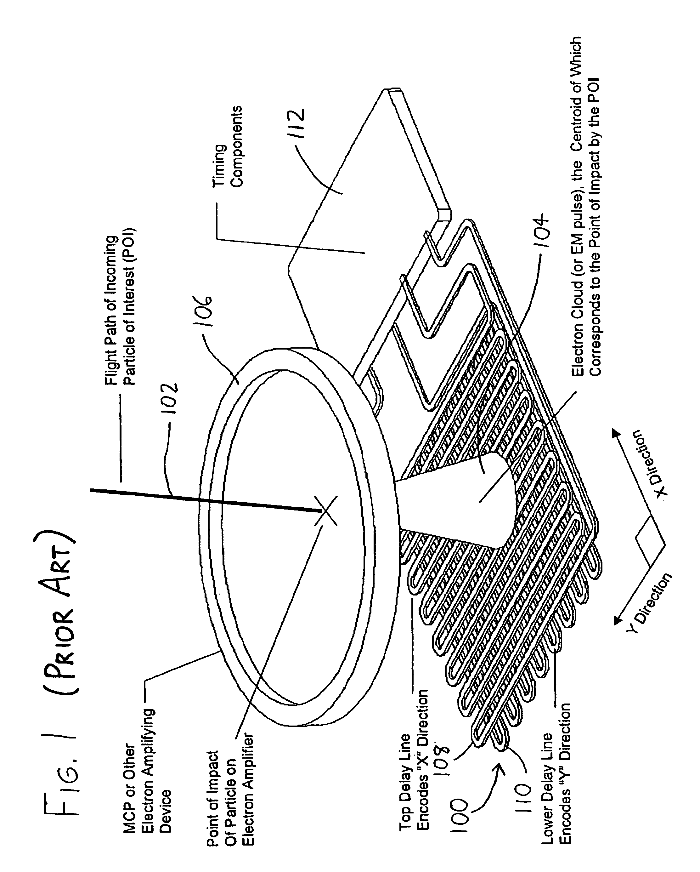
Apart from the timing components, the delay line anode can affect detector accuracy by affecting the size and sharpness of the input EMP into the timing components through attenuation, and also by impedance mismatch between the anode and the timing components.
Impedance mismatch reduces the speed at which the detector can record events because mismatch causes reflections of the EMP at the point of mismatch.
Similarly, unless precautions are taken, the reflected EMP may create a spurious timing event at the other end of the delay line.
A primary disadvantage of this fabrication method is the need to remove multiple layers of dielectric material 208 and 222 by laser ablation machining in order to expose the lower anode 210 and its signal line 212.
This machining is difficult and expensive, particularly owing to the high aspect ratio (ratio of depth to width)—approximately 4:1 —of the channels of dielectric that are ablated.
The need for deep cutting significantly heats the board, often resulting in warping and imperfect production unless cutting is done in multiple stages, which greatly increases manufacturing time and cost.
Apart from problems with the fabrication method, there are numerous disadvantages with the structural features of anodes made by the foregoing method.
First, the resulting anode array detector is often incompatible with Ultra High Vacuum (UHV) environments.
The detector is fabricated using standard printed circuit board techniques and materials, but standard circuit board materials are incompatible with UHV environments due to insufficient temperature stability and outgassing.
Most typical printed circuit board materials are stable at temperatures up to approximately 120° C.; however, UHV environments typically require that materials be stable to approximately 150°–200° C. In addition, most adhesives and circuit board materials used in traditional printed circuit board manufacture continuously release gas, and this is similarly unsuitable for use in UHV environments.
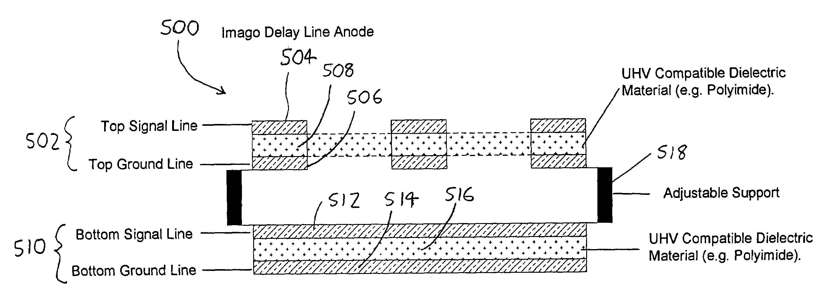
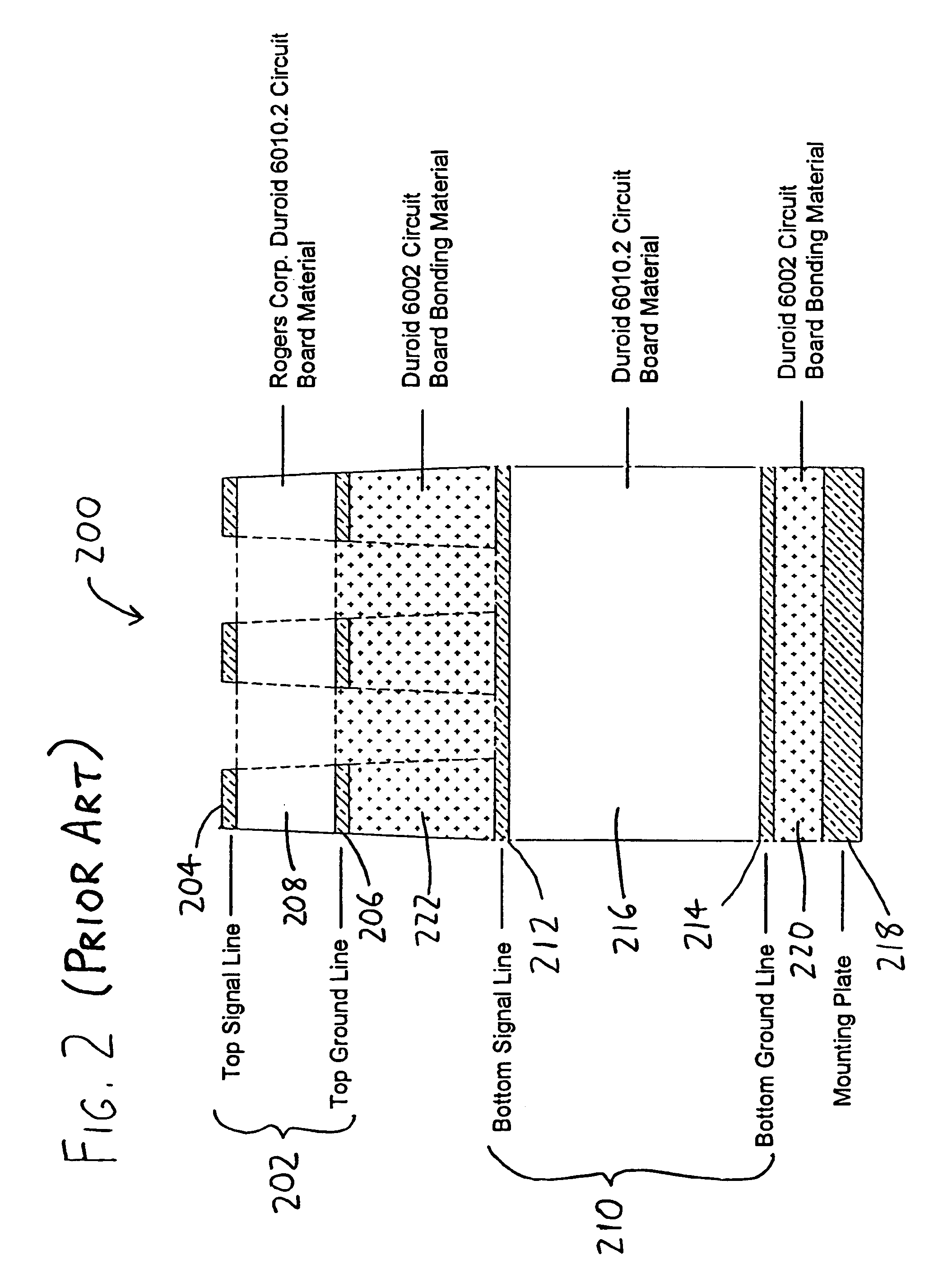
Second, the need to bond the two anodes / boards 202 and 210 together results in undesirable nonuniformity in detector properties.
As a result, the impedance of the lower signal line 212 will be difficult to accurately control, thus causing problems with impedance matching to the timing components 112 and other components.
As one might expect, if the upper and lower signal lines 204 and 212 display different performance characteristics—as they almost inevitably will do—the complexity of the timing components 112 grows and results become more difficult to interpret.
This precludes efficient mass production of a complete detector assembly.
Third, the permanence of the bond between the two anodes 204 and 210 is also disadvantageous in that if one anode is found to be defective after bonding to the other anode, the entire detector must be scrapped.
This potentially results in discarding a non-defective anode along with the defective one, thereby increasing losses from wasted time and materials.
Fourth, detector accuracy is partially dependent on alignment of the two delay lines in a known orientation—typically 90°—but the nature of the bonding process used to bond the upper and lower anodes 202 and 210 together makes precise positional registration between their delay lines difficult to achieve.
Further, since bonding renders the anode alignment permanent, deviations from the desired alignment cannot be corrected after the bonding is completed.
Fifth, the active area of a standard printed circuit board anode (i.e., the area over which the delay line receives particles) is practically limited by the resistance of delay lines having widths achievable with standard printed circuit board fabrication methods, which is typically 60 microns or less.
If delay lines are thinner, more may be fit within any given active area; however, thinner lines have higher electrical resistance, and thus can exhibit undesirable characteristics (in particular higher attenuation).
Sixth, anodes fabricated using standard printed circuit board techniques are generally limited to a planar form.
If it is desirable to have a nonplanar or otherwise irregularly-shaped anode, or an anode with changeable configuration, the foregoing scheme seems inapplicable as a practical matter because the etching, bonding, ablation, etc. are difficult to economically perform on non-planar boards.
Seventh, the foregoing fabrication scheme gives rise to limitations in the resulting anode.
Although this scheme eliminates the problems of laser ablation, the vias add cost and complexity to the fabrication process.
Further, each via adds a capacitive load to the signal line, thus significantly altering its electrical properties (generally decreasing impedance and pulse amplitude, and slowing propagation speed).
Finally, the vias act as miniature antennae between the two signal lines, increasing crosstalk between lines and dissipation of the signal, which ultimately decreases the overall performance of the anodes.
To summarize, prior delay line anode fabrication methods are difficult and costly to execute, and they yield multi-anode detectors wherein the component anodes display significantly different electrical characteristics, thereby complicating electronics and interconnection issues and ultimately limiting detector performance.

Method used


Image

  • Delay line anodes
  • Delay line anodes
  • Delay line anodes

Examples


Embodiment Construction

[0039]A first preferred version of the invention will now be described with reference to FIG. 3, wherein an exemplary single delay line anode 300 is shown in an exploded view. The anode 300 includes an upper signal line layer 302, a middle dielectric layer 304, and a bottom ground layer 306 shown in spaced relation (with a portion of the dielectric layer 304 cut away so that the ground layer 306 is more easily viewed). The upper signal line layer 302 and bottom ground layer 306 are formed of pre-patterned metal foils cut into the illustrated configuration by die cutting, laser cutting, water jet cutting, or other material removal processes, including etching and photolithographic processes. It is noted that laser cutting and etching processes are not as disadvantageous for the anode 300 as they are in prior art anode manufacturing processes since the foils used to form the signal line layer 302 and ground layer 306 may be thicker than the conductive layers in standard printed circui...


PUM


Abstract

In detectors for imaging and other applications, delay line anodes are arrayed so as to allow detection of the location and/or timing of particle hits. The anodes are arrayed to provide an upper anode and one or more lower anodes, with particles incident on the upper anode passing in turn to the lower anodes. The anode arrays allow the use of identically manufactured anodes which are maintained in parallel spaced relation along the travel path of the particles of interest without dielectric material or other structure situated between the anodes. The spacing between the anodes is preferably adjustable so as to allow the installer and/or user to modify the performance characteristics of the array. The anodes may be made of pre-formed metal foil signal and ground layers laminated onto opposing sides of a dielectric sheet, or may be etched or otherwise formed from flex circuit material, so that the anodes and the overall array are light weight, compact, and flexible.

Description

CROSS-REFERENCE TO RELATED APPLICATIONS[0001]This application claims priority under 35 USC § 119(e) to U.S. Provisional Patent Application 60 / 213,801 filed 26 Jun. 2000, the entirety of which is incorporated by reference herein.FIELD OF THE INVENTION[0002]This disclosure concerns an invention relating generally to delay line anodes, and more specifically to methods for fabricating delay line anodes and delay line anode arrays with improved electrical properties, particularly delay line anode arrays employed in time- and position-sensitive particle detectors such as those used in imaging applications.BACKGROUND OF THE INVENTION[0003]Delay line anodes are apparata used in time- and / or position-sensitive detectors to encode the time and position of impact of particles (e.g., electrons, atoms, ions, molecular complexes, etc.) and / or photons incident upon the detector. The function and operation of delay line anodes in such detectors is briefly described here to provide the reader with a...

Claims


Application Information

Patent Timeline
Patent Type & Authority Patents(United States)
IPC IPC(8): G01T3/00
CPCG01T1/2957
Inventor GRIBB, TYE TRAVISLARKIN, JOHN JOSEPH
Owner CAMECA INSTR
Why Eureka
Try Eureka