Light-emitting diode array

Inactive Publication Date: 2009-03-17
LEXTAR ELECTRONICS CORP
View PDF8 Cites 18 Cited by
  • Summary
  • Abstract
  • Description
  • Claims
  • Application Information

AI Technical Summary

Benefits of technology

[0015]In the light-emitting diode array of the present invention, the light-emitting portions and the bonding portions are preferably formed by separating or dividing epitaxial layers formed on the conductive layer by mesa-etched grooves. In the light-emitting diode array according to a preferred embodiment, the bonding pads are formed on separate bonding portions, so that there is no short-circuiting between the bonding pads eve

Problems solved by technology

Because the lift-off method has insufficient step coverage, wiring layers in LEDs having large mesa-etched steps are easily broken at the steps.
Though wiring layers formed by the sputtering/ion-milling method have good step coverage and are resistant to breakage at the steps, Au disadvantageously tends to remain at the mesa-etched steps.
Particularly, LEDs of the dynamic driving system comprising common electrodes are disadvantageous in the short-circuiting of wir

Method used


Image

  • Light-emitting diode array
  • Light-emitting diode array
  • Light-emitting diode array

Examples


Example

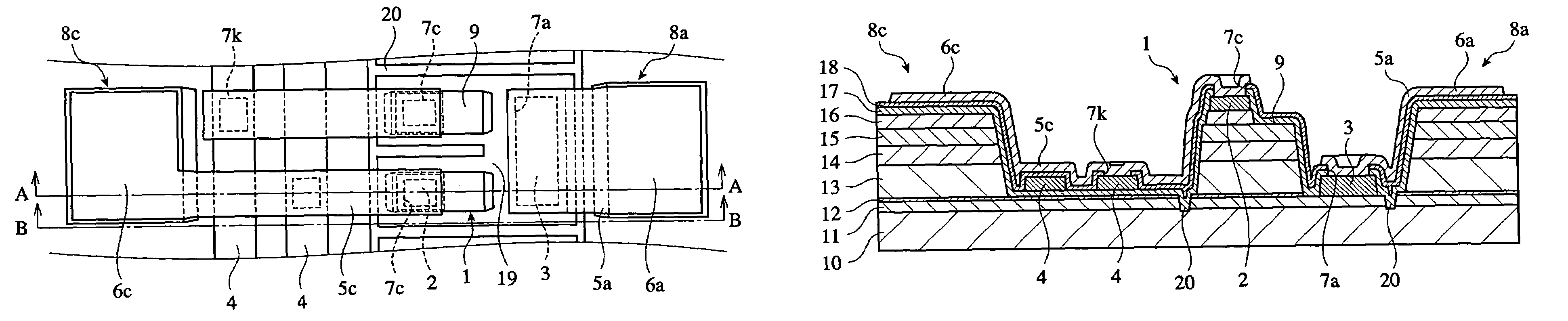
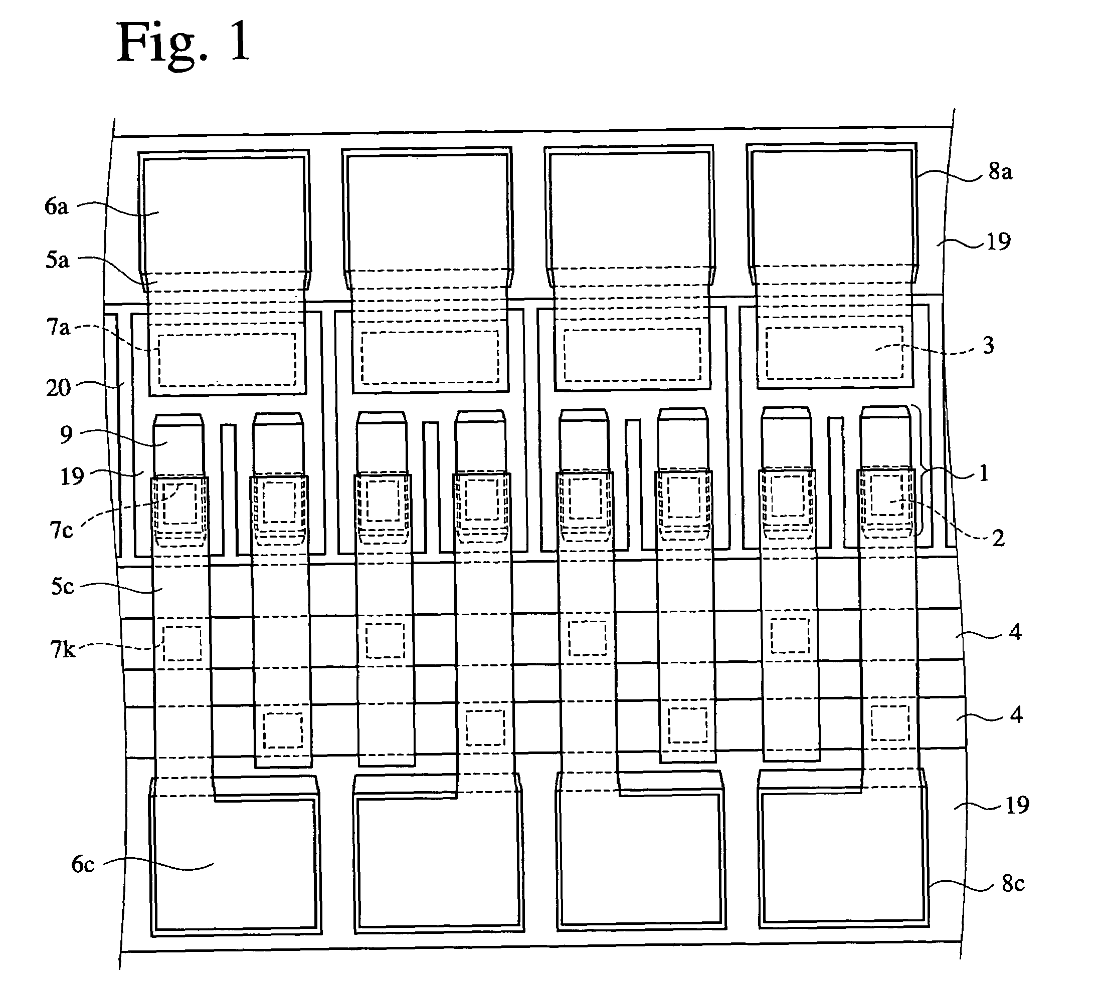
[1] Structure of Light-emitting Diode Array

[0026]As shown in FIGS. 1 and 2, the light-emitting diode array of the present invention comprises a substrate 10, a plurality of light-emitting portions 1 formed on the substrate 10, a first electrode 2 partially formed on a top surface of each light-emitting portion 1, and a second electrode 3 formed on the conductive layer 11 adjacent to the light-emitting portions 1. In the depicted embodiment, each light-emitting portion 1 is a separate epitaxial layer portion obtained by dividing an epitaxial layer uniformly formed on the substrate 10 by mesa-etched grooves 19, 20.

(1) Substrate

[0027]The substrate 10 is not particularly restrictive as long as it may be used for light-emitting diodes, and it need only have a structure capable of electrically insulating the light-emitting parts. It may be either an n-type substrate or a p-type substrate, and a semi-insulating substrate such as a semi-insulating GaAs substrate, etc. or an insulating subst...


PUM


Abstract

A light-emitting diode array comprising a conductive layer formed on a substrate, separate light-emitting portions formed on the conductive layer, a first electrode formed on at least part of an upper surface of each light-emitting portion, and a second electrode formed on the conductive layer adjacent to the light-emitting portions; the first electrode comprising a common switching electrode matrix; the second electrode comprising a common electrode divided such that one second electrode exists in every block; and at least one of bonding pads extending to the first common electrode and the second common electrode being formed on a bonding portion formed on the conductive layer like an island, whereby the bonding pads are separate from each other.

Description

FIELD OF THE INVENTION[0001]The present invention relates to a light-emitting diode array of high emission power, and particularly to a light-emitting diode array suitable for light sources of electrophotographic printers.BACKGROUND OF THE INVENTION[0002]An electrophotographic printer forms an electrostatic latent image on a photosensitive drum by light according to an image signal, develops the latent image by selectively attracting toner thereto, and then transfers the developed image onto a paper to obtain a print image. As a light source for forming the electrostatic latent image, a laser and a light-emitting diode array are widely used. In particular, since a light source constituted by the light-emitting diode array does not need a long optical path unlike the laser-type light source, it is suitable for small-sized printers and large-sized printing. Demand has been mounting recently on light-emitting diode arrays of higher precision, higher emission power and low in cost, as p...

Claims


Application Information

Patent Timeline
IPC IPC(8): H05B33/04H01L29/18H05B33/10H01L33/00B41J2/44B41J2/45H01L27/15H01L33/08H01L33/20H01L33/30H01L33/40H01L33/44H01S5/00
CPCH01L27/153B41J2/45B65H75/28B65H75/30B65H75/4444B65H2701/34H02G11/02
Inventor YUKIMOTO, TOMIHISAKUNITAKE, EIICHISUGIYAMA, SATOSHIKOMORI, YOSUKESUKEGAWA, TOSHIMITSU
Owner LEXTAR ELECTRONICS CORP
Why Eureka
Try Eureka