Method of determining a flatness of an electronic device substrate, method of producing the substrate, method of producing a mask blank, method of producing a transfer mask, polishing method, electronic device substrate, mask blank, transfer mask, and polishing apparatus

a technology of electronic devices and substrates, which is applied in the direction of magnetic recording, chemical vapor deposition coating, and recording information storage. it can solve the problems of pattern displacement errors or pattern defects, deterioration of the total flatness of the photomask blank as a material of the photomask, and deterioration of the pattern position accuracy. achieve the desired flatness of the mask blank and the desired flatness of the transfer mask, and avoid deterioration of the pattern position accuracy of the transfer mask

Inactive Publication Date: 2005-10-04
HOYA CORP
View PDF9 Cites 30 Cited by
  • Summary
  • Abstract
  • Description
  • Claims
  • Application Information

AI Technical Summary

Benefits of technology

[0017]It is therefore an object of this invention to provide a method of producing a mask blank including a thin film and a method of producing a transfer mask having a pattern, which are capable of achieving a desired flatness of the mask blank and a desired flatness of the transfer mask even if the thin film itself has a film stress and which are capable of avoiding deterioration in pattern position accuracy of the transfer mask as well as occurrence of a pattern displacement error and a pattern defect during pattern transfer.

Problems solved by technology

Although such a high flatness of the transparent substrate is achieved as described above, the total flatness of a photomask blank as a material of the photomask is deteriorated by the thin film formed on the transparent substrate because the thin film itself has a film stress.
The deterioration in total flatness of the photomask blank results in degradation of a pattern position accuracy when the thin film is patterned and the photomask is produced.
Accordingly, when the pattern is transferred onto the semiconductor wafer, a pattern displacement error or a pattern defect will be caused to occur.
However, in a recent semiconductor integrated circuit more and more increased in density and accuracy, such a reduced film stress of the thin film is yet unnegligible.
It is therefore difficult to control the film stress of the thin film.
This results in degradation of a pattern position accuracy when the thin film is patterned and the photomask is produced.
Accordingly, when the pattern is transferred onto the semiconductor wafer, a pattern displacement error or a pattern defect will be caused to occur.
However, it is difficult to maintain an accuracy of the surface table within a wide plane of the surface table.
As described above, however, it is difficult to achieve a high-flatness substrate having a flatness not greater than 0.25 μm and adapted to be used as a substrate for a (ArF, F2, EUV) mask corresponding to the design rule of the next-generation semiconductor integrated circuit.
Because of change in polishing condition (such as deterioration of the polishing pad and the abrasive grains) and because of the batch-type polishing method, it is difficult to produce a mask blank substrate at a high yield even if the flatness is between 0.5 μm and 1 μm.
However, in the above-mentioned polishing method using the double-sided polishing apparatus, the flatness has a limit of about 1 μm.
However, for a thick substrate, such as a mask blank substrate, having a thickness of 6.5 mm (in case of a 6-inch substrate), the above-mentioned polishing apparatus can not effectively adjust the flatness of the substrate because the pressing force is insufficient.
Therefore, the pressing force is difficult to control.

Method used


Image

  • Method of determining a flatness of an electronic device substrate, method of producing the substrate, method of producing a mask blank, method of producing a transfer mask, polishing method, electronic device substrate, mask blank, transfer mask, and polishing apparatus
  • Method of determining a flatness of an electronic device substrate, method of producing the substrate, method of producing a mask blank, method of producing a transfer mask, polishing method, electronic device substrate, mask blank, transfer mask, and polishing apparatus
  • Method of determining a flatness of an electronic device substrate, method of producing the substrate, method of producing a mask blank, method of producing a transfer mask, polishing method, electronic device substrate, mask blank, transfer mask, and polishing apparatus

Examples


example 5

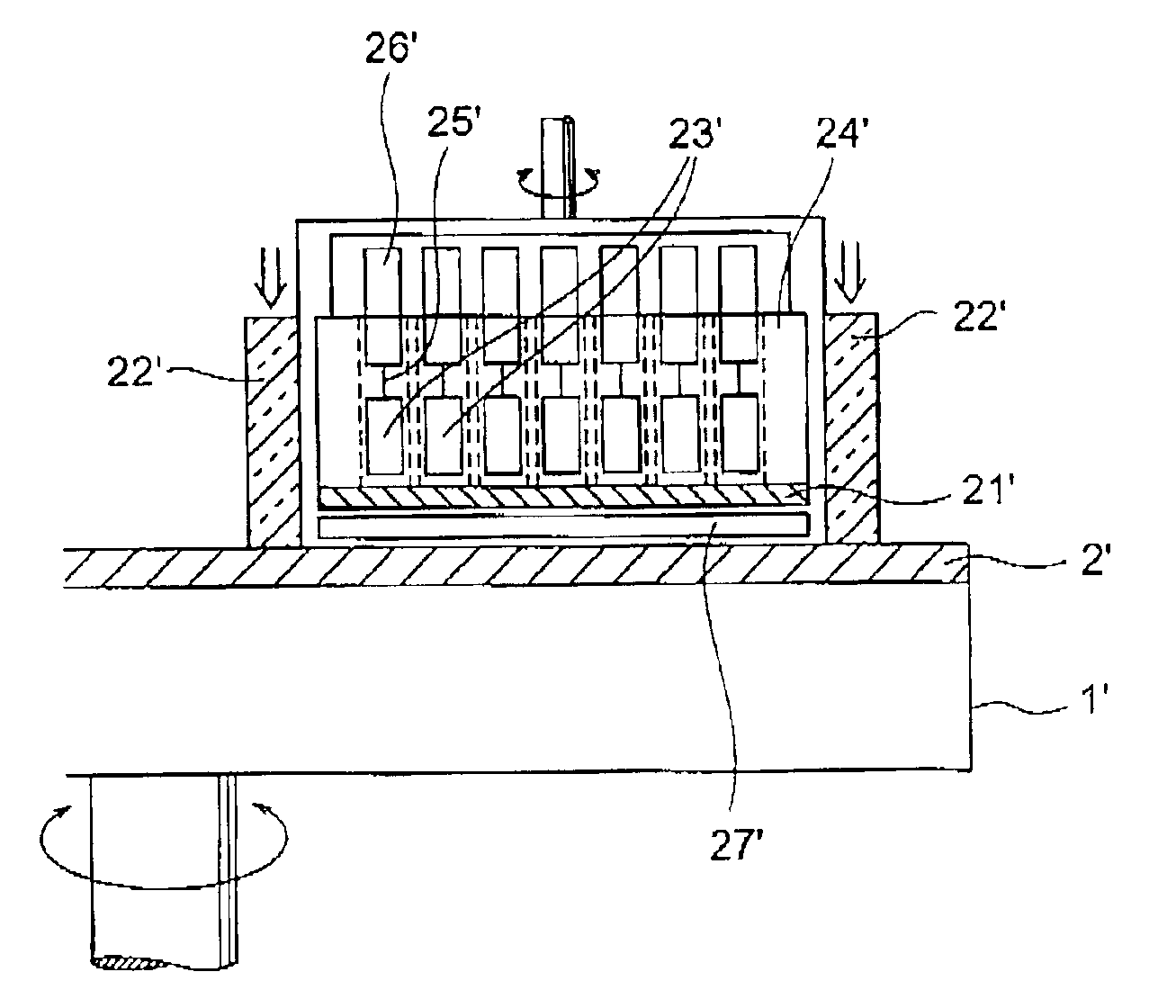
[0230]Referring to FIG. 5, the flatness of the electronic device substrate of a concave shape was adjusted.

[0231]As a result of measurement of the electronic device substrate, the substrate surface had a profile like a bowl. The flatness was within a range between 0.6 and 0.7 μm (concave). Therefore, the load type (3) in which corner portions of the substrate are applied with higher pressure is at first selected. More in detail, no load was applied upon the pressing members 3 disposed at the center portion of the substrate while the pressing members 3 disposed at the corner portions of the substrate were applied with a highest load. In FIG. 5, numerical values shown in the load types (3) and (4) represent the pressure (kg / cm2) exerted upon the substrate. The substrate was polished at the rotation speed of 10-20 rpm for a polishing time of 45-100 seconds. Use was made of a polishing solution containing colloidal silica (average particle size of 100 nm) as an abrasive suspended in wat...

example 6

[0234]The flatness was adjusted in the manner similar to Example 3 except that the polishing solution in Example 3 was replaced by a polishing solution containing colloidal silica (average particle size of 100 nm) as an abrasive and sodium hydroxide added thereto so as to achieve a pH value of 11.2 and that mechanochemical polishing was used.

[0235]As a result, the substrate finally obtained had a substantially equivalent flatness. However, the polishing time required in adjustment of the flatness can be shortened by about 15-20%.

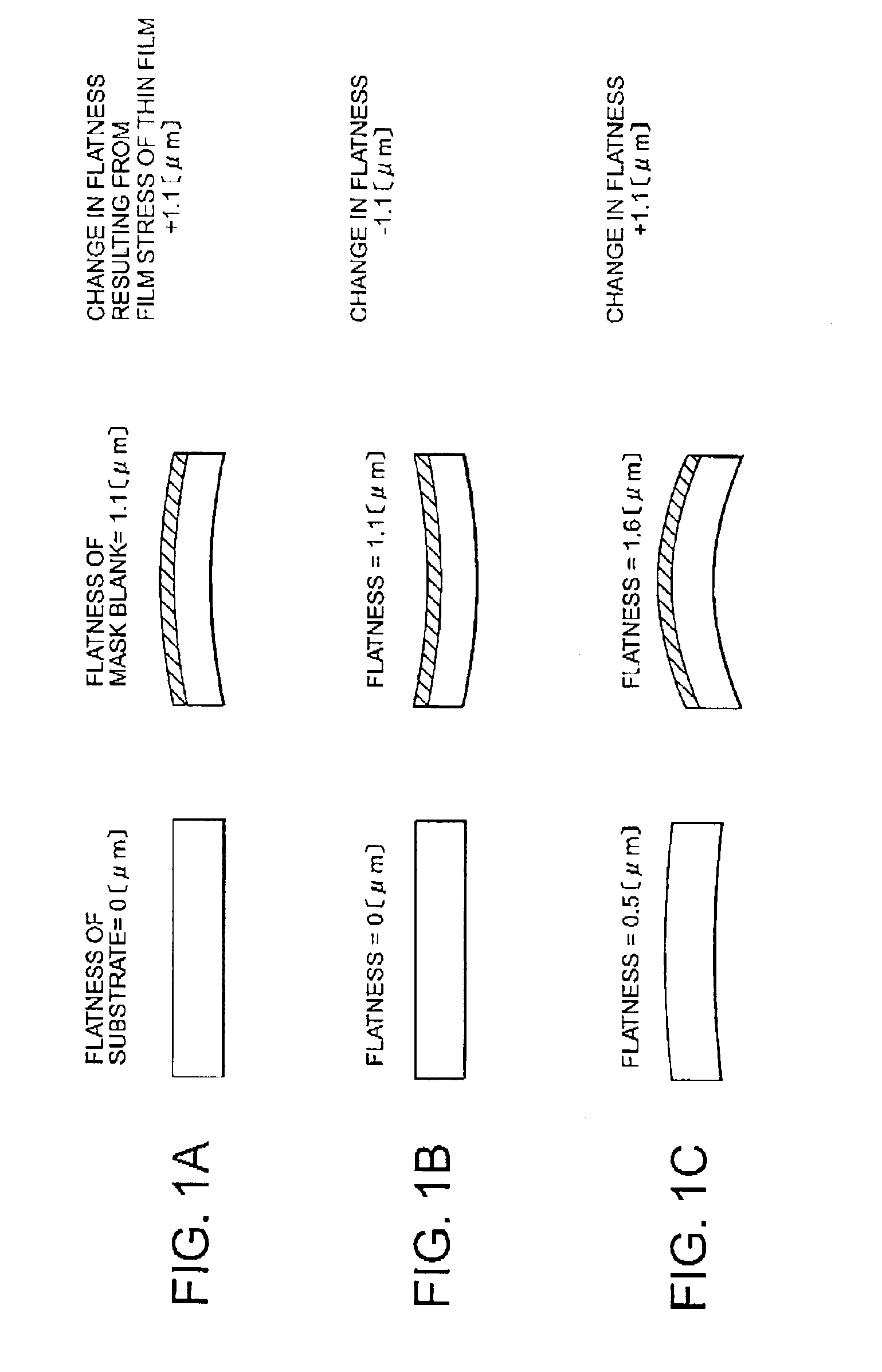
[0236]According to this invention, even in case where the thin film itself has a film stress, the photomask blank having a desired flatness can be obtained. It is therefore possible to provide a method of producing a photomask blank and a method of producing a photomask, which are capable of achieving a desired flatness of the photomask blank and which are capable of avoiding deterioration in pattern position accuracy of the photomask as well as occurrence o...

example 1

[0284]1) Rough Polishing Step (S101)

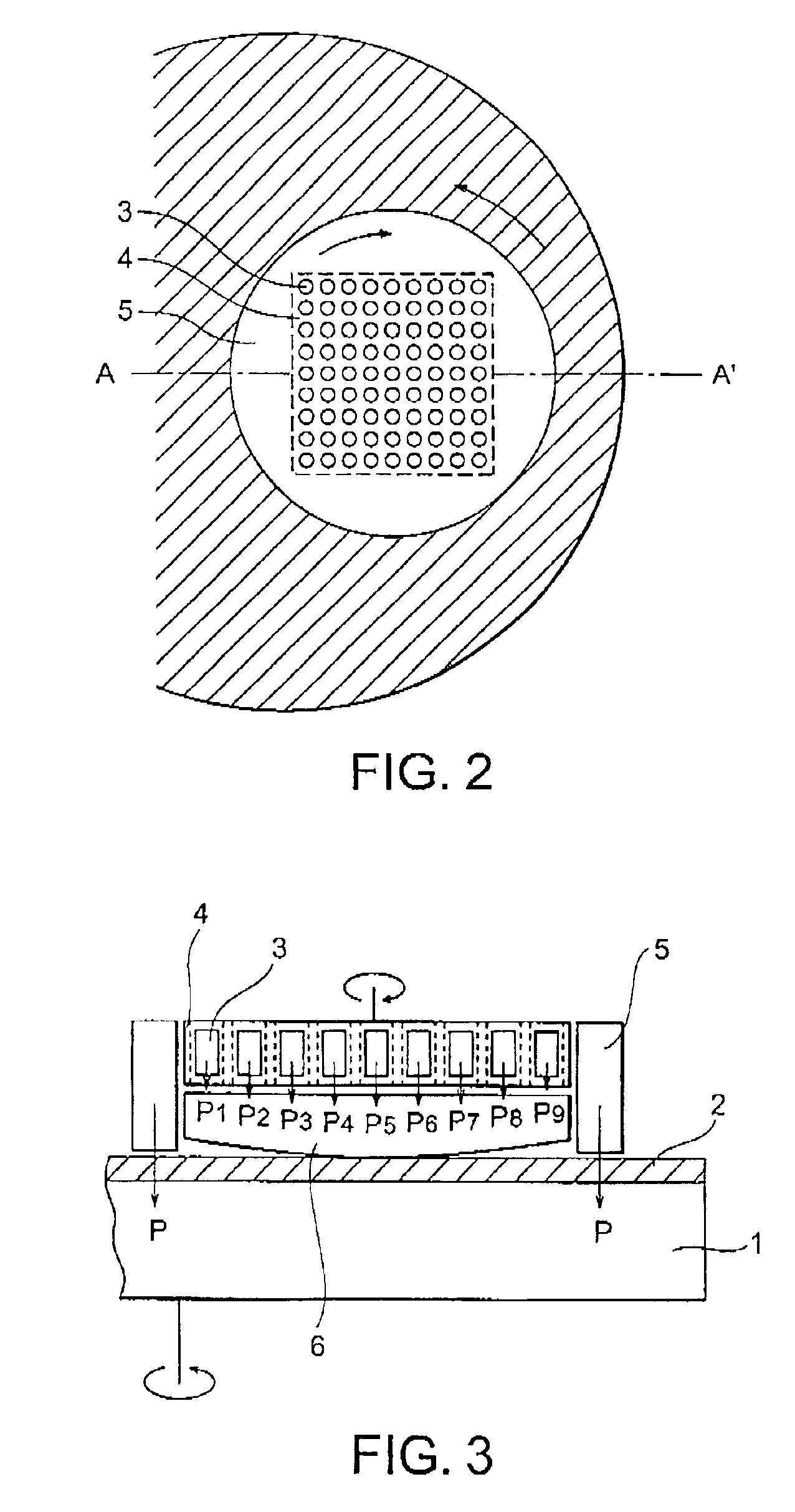
[0285]Preparation was made of synthetic quartz glass substrates (6 inch×6 inch) after subjected to chamfering at its end faces and lapping by a double-sided lapping apparatus. The glass substrates, 12 in number, were set in the above-mentioned double-sided polishing apparatus and subjected to a rough polishing step in the following polishing condition. A working load and a polishing time were appropriately adjusted.

[0286]

Polishing Solution:cerium oxide (average particle size: 2-3 μm) +waterPolishing Pad:hard polisher (urethane pad)

[0287]After completion of the rough polishing step, the glass substrates were dipped in a cleaning tank (applied with an ultrasonic wave) to be cleaned in order to remove abrasive grains adhered to the glass substrates.

[0288]2) Precision Polishing Step (S101)

[0289]The glass substrates, 12 in number, were set in the above-mentioned double-sided polishing apparatus and subjected to a precision polishing step in the followi...


PUM

PropertyMeasurementUnit
flatnessaaaaaaaaaa
flatnessaaaaaaaaaa
surface roughness Raaaaaaaaaaa

Abstract

A flatness of a substrate is determined to achieve a desired flatness of a mask blank by predicting the variation in flatness resulting from a film stress of a thin film formed on the substrate. The flatness is adjusted by measuring the flatness of the substrate as a measured flatness, selecting a load type with reference to the measured flatness, and polishing the substrate under pressure distribution specified by the load type. A principal surface of the substrate has a flatness greater than 0 μm and not greater than 0.25 μm. A polishing apparatus includes a rotatable surface table, a polishing pad formed thereon, abrasive supplying means for supplying an abrasive to the polishing pad, substrate holding means, and substrate pressing means for pressing the substrate. The substrate pressing means has a plurality of pressing members for individually and desirably pressing a plurality of divided regions of the substrate surface.

Description

BACKGROUND OF THE INVENTION[0001]This invention relates to a method of determining a flatness of an electronic device substrate used in a mask blank, a method of producing the substrate adjusted in flatness, a method of producing a mask blank, a method of producing a transfer mask, and a polishing method. This invention also relates to an electronic device substrate (such as a mask blank substrate) having a high flatness and a high parallelism, a mask blank and a transfer mask using the substrate, and a polishing apparatus.[0002]Upon production of a semiconductor integrated circuit device, a photolithography technique is used in a process of forming a wiring region and other various regions. In a photolithography process using the photolithography technique, a photomask is used as an original pattern for exposure. The photomask comprises a transparent substrate and a light shielding thin film formed thereon and having a pattern. The pattern of the light shielding thin film is transf...

Claims


Application Information

Patent Timeline
Patent Type & Authority Patents(United States)
IPC IPC(8): C23C14/34B24B49/02B24B49/16B24B37/04B24B49/04B24B41/06G03F1/14G03F7/20B24B37/30G03F1/00
CPCB24B37/30B24B49/04G03F1/14B24B49/16Y10T428/24355G03F1/60G03F9/7034G03F1/62
Inventor KOIKE, KESAHIROOHTSUKA, MASATOTOCHIHARA, YASUTAKA
Owner HOYA CORP
Why Eureka
Try Eureka