Microelectromechanical device with integrated conductive shield

a microelectromechanical and shield technology, applied in the direction of microstructural devices, acceleration measurement using interia forces, fluid pressure measurement, etc., can solve the problems of device electrical output and device's inability to achieve acceptable performance levels

Inactive Publication Date: 2005-10-04
HONEYWELL INT INC
View PDF5 Cites 54 Cited by
  • Summary
  • Abstract
  • Description
  • Claims
  • Application Information

AI Technical Summary

Benefits of technology

[0008]According to one embodiment, a semiconductor microelectromechanical device, such as a pressure sensor or accelerometer, may include a substrate over which a sensing element is formed. A conductive shield may be fabricated over at least a portion of the sensing element. Further, the conductive shield ma

Problems solved by technology

Environmental conditions acting on or impressed upon environmentally susceptible microelectromechanical devices may cause unwanted effects that may prevent the devices from attaining acceptable

Method used


Image

  • Microelectromechanical device with integrated conductive shield
  • Microelectromechanical device with integrated conductive shield
  • Microelectromechanical device with integrated conductive shield

Examples


Embodiment Construction

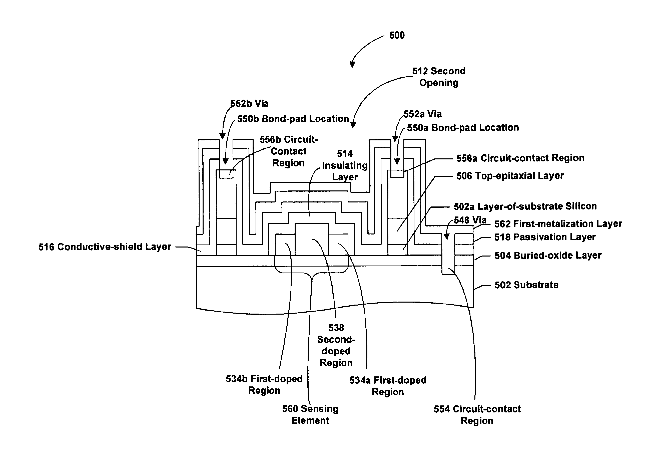
[0017]The embodiments of the microelectromechanical device described herein are described in relation to a preferred microelectromechanical pressure sensor and its architectural components. The described architecture and processes for fabricating the microelectromechanical pressure sensor are likewise applicable to other microelectromechanical devices.

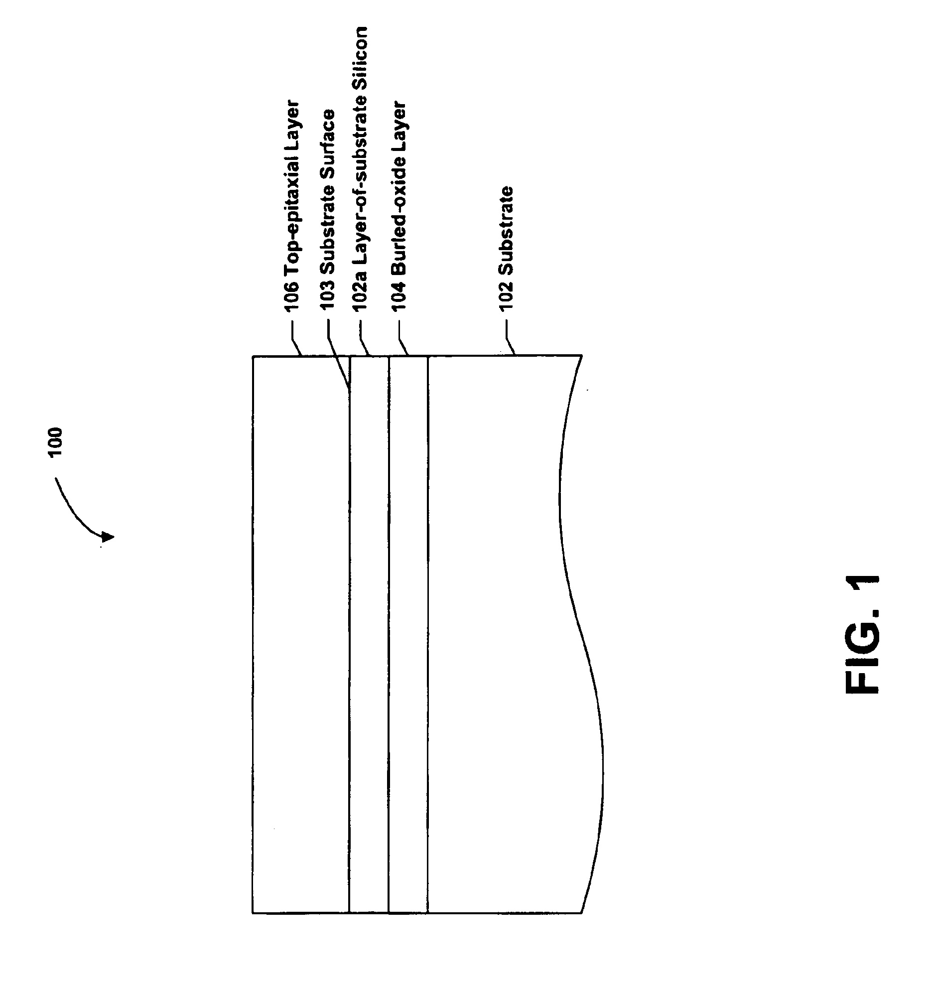
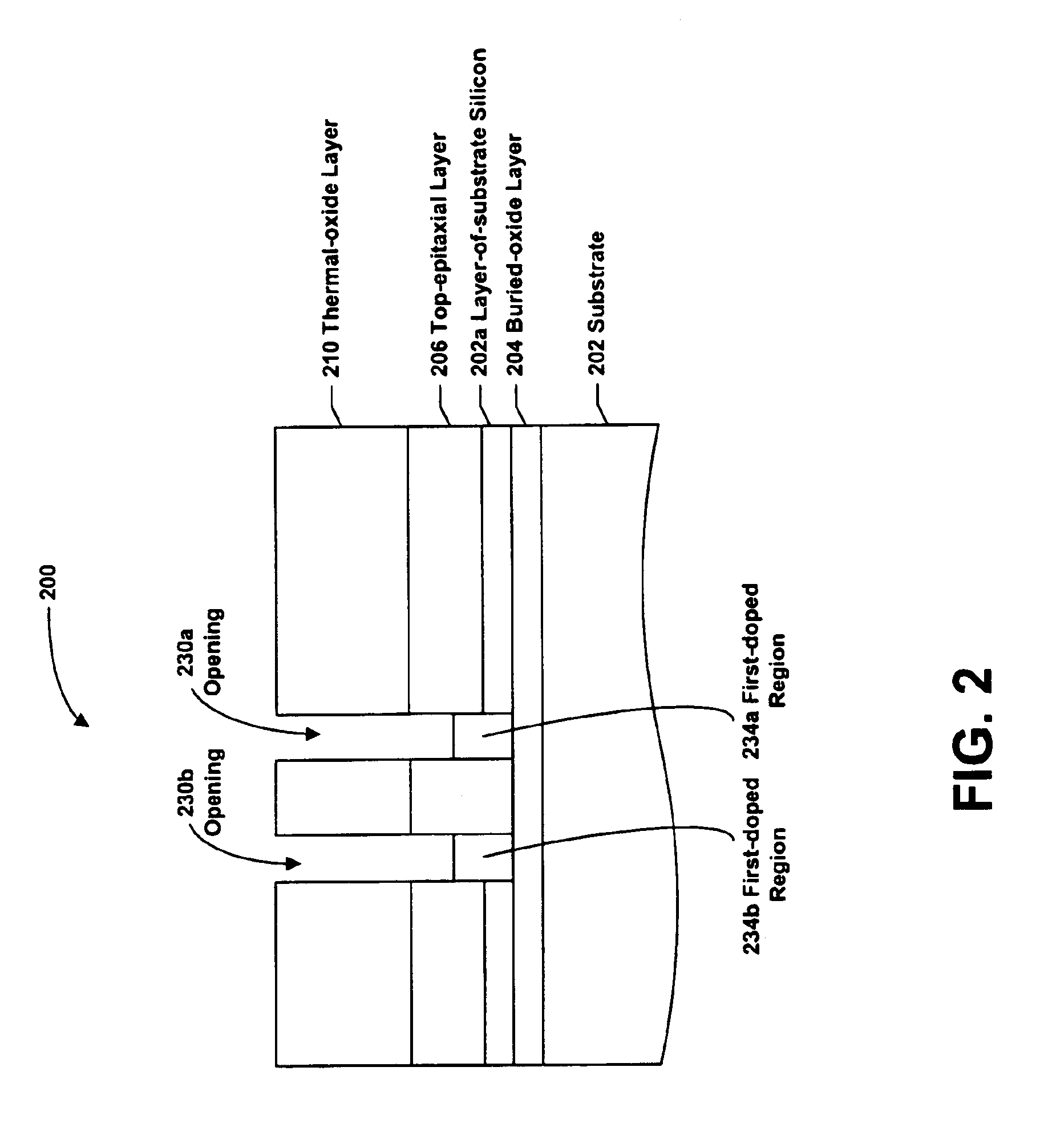
[0018]FIG. 1 is a conceptual drawing illustrating an embodiment of a cross-section of the substructure of a microelectromechanical device 100 at a first processing phase. While FIG. 1 and other subsequent figures illustrate the microelectromechanical device's substructure at certain processing phases, these phases are for illustration purposes only and not necessarily intended to limit the scope of the present embodiments, provide sequential processing steps, or provide an inflexible fabrication recipe.

[0019]Referring to FIG. 1, the microelectromechanical device 100 includes a substrate 102, a layer-of-substrate silicon 102a, a buried-...


PUM

PropertyMeasurementUnit
Temperatureaaaaaaaaaa
Fractionaaaaaaaaaa

Abstract

A microelectromechanical device and method of fabricating the same, including a layer of patterned and deposited metal or mechanical-quality, doped polysilicon inserted between the appropriate device element layers, which provides a conductive layer to prevent the microelectromechanical device's output from drifting. The conductive layer may encapsulate of the device's sensing or active elements, or may selectively cover only certain of the device's elements. Further, coupling the metal or mechanical-quality, doped polysilicon to the same voltage source as the device's substrate contact may place the conductive layer at the voltage of the substrate, which may function as a Faraday shield, attracting undesired, migrating ions from interfering with the output of the device.

Description

FIELD[0001]The present invention is related to integrated microelectromechanical devices and more particularly, to semiconductor microelectromechanical devices with an integrated conductive shield, and a method for manufacturing the same.BACKGROUND[0002]Microelectromechanical devices are useful in many applications. These devices range from automobile sensors to actuators used on space exploration vehicles. Generally, these sensors and actuators provide information about environmental conditions, and / or react to changes in the environmental conditions. For instance, a microelectromechanical-pressure-sensor device may be used to measure an automobile's engine manifold pressure (or vacuum). In operation, the microelectromechanical-pressure-sensor device provides an electrical output that is proportional to the manifold pressure (or vacuum). This electrical output may be used by an engine management system for controlling fuel delivery to the automobile's engine.[0003]In another useful...

Claims


Application Information

Patent Timeline
IPC IPC(8): G01L9/00G01L19/06B81C1/00B81B7/02
CPCG01L9/0042G01L19/0627
Inventor STRATTON, THOMAS G.GARDNER, GARY R.RAHN, CURTIS H.
Owner HONEYWELL INT INC
Why Eureka
Try Eureka