Color liquid crystal display

a liquid crystal display and color technology, applied in the field of liquid crystal display, can solve the problem of degrading the contrast of the lcd, and achieve the effect of high contras

Inactive Publication Date: 2005-10-04
SANYO ELECTRIC CO LTD
View PDF14 Cites 5 Cited by
  • Summary
  • Abstract
  • Description
  • Claims
  • Application Information

AI Technical Summary

Benefits of technology

[0019]In light of the above, the object of the present invention is to provide a LCD with high contrast wherein a data line is formed overlapping pixel electrodes.
[0022]According to the above arrangement of the present invention, color filters are formed in an interlayer between a data line and pixel electrodes in a liquid crystal display having the data line disposed overlapping the pixel electrodes. Space is thereby provided between the data line and the pixel electrodes, reducing parasitic capacitance between the data line and the pixel electrodes. Accordingly, changes in pixel electrode potentials can be suppressed to enable application of sufficient voltage to those pixel electrodes, thereby realizing a color liquid crystal display with high contrast.
[0028]In a liquid crystal display having orientation controllers comprising components such as orientation control windows or orientation control slope faces, a plurality of orientation directions of liquid crystal can be set within a single pixel using the orientation controllers to broaden the viewing angle of the display. By adopting such a structure, a high-contrast, high-quality display having reduced parasitic capacitance between a data line and pixel electrodes can be accomplished with a broad viewing angle.
[0032]When a data line is arranged overlapping orientation control windows, data line wiring tends to become longer compared to when the data line is arranged without overlapping the orientation control windows, further increasing parasitic capacitance between the data line and the pixel electrodes. By providing color filters in an interlayer between the data line and the pixel electrodes according to the present invention to reduced the parasitic capacitance, degradation of contrast resulting from increased wiring length of the data line can be prevented. Degradation of contrast due to lengthy wiring of the data line can be prevented by disposing color filters in an interlayer between the data line and the pixel electrodes similarly in a LCD wherein the positions of the orientation control slope faces and the data line are overlapped.
[0034]In a device of the present invention wherein a switch element is formed, for example, in an underlying layer of each of the plurality of pixel electrodes, presence of a color filter in each contact region between the switch element and the pixel electrode may require special processes to maintain a favorable connection between the switch element and the pixel electrode positioned over the color filter. When at least a color filter is positioned between the switch element and the pixel electrode, the contact hole for connecting the pixel electrode and the switch element must have a depth passing through the color filter, and this requirement is disadvantageous in obtaining a reliable contact. Moreover, when adopting a manufacturing method in which, before forming the color filter, a contact hole is initially created in an interlayer insulating film formed covering the switch element, color filter material may enter into the created contact hole. Connection between the pixel electrode and the switch element may become deficient if this material is not completely removed from the hole. In light of this situation, formation of a reliable contact between the switch element and the pixel electrode is facilitated by eliminating presence of the color filter in the contact region between the switch element and the pixel electrode.
[0037]Operation of liquid crystal is controlled by the potential difference between pixel electrodes and the opposing common electrode. To efficiently apply a voltage to the liquid crystal, it is preferable to dispose the pixel electrodes on the first substrate as close to the liquid crystal as possible. Accordingly, when forming the structure having color filters located in a layer between the pixel electrodes and the data line, the data line is disposed closer to the first substrate, while the pixel electrodes are formed in an overlying layer. In this way, pixel electrodes can be provided closer to the liquid crystal.

Problems solved by technology

The contrast of the LCD would then degrade due to insufficient driving of the liquid crystal.
In addition, when in the “normally black mode”, the liquid crystal beneath an orientation control window 63 does not allow light to pass through even during voltage application because its initial orientation is maintained.
This problem may similarly exist when a data line is formed overlapping pixel electrodes in LCDs other than ones having orientation control windows, such as a LCD with slope portions disposed on an orientation film contacting the liquid crystal for orientation control described in the above-mentioned JPA H07-311383.

Method used


Image

  • Color liquid crystal display
  • Color liquid crystal display
  • Color liquid crystal display

Examples


Embodiment Construction

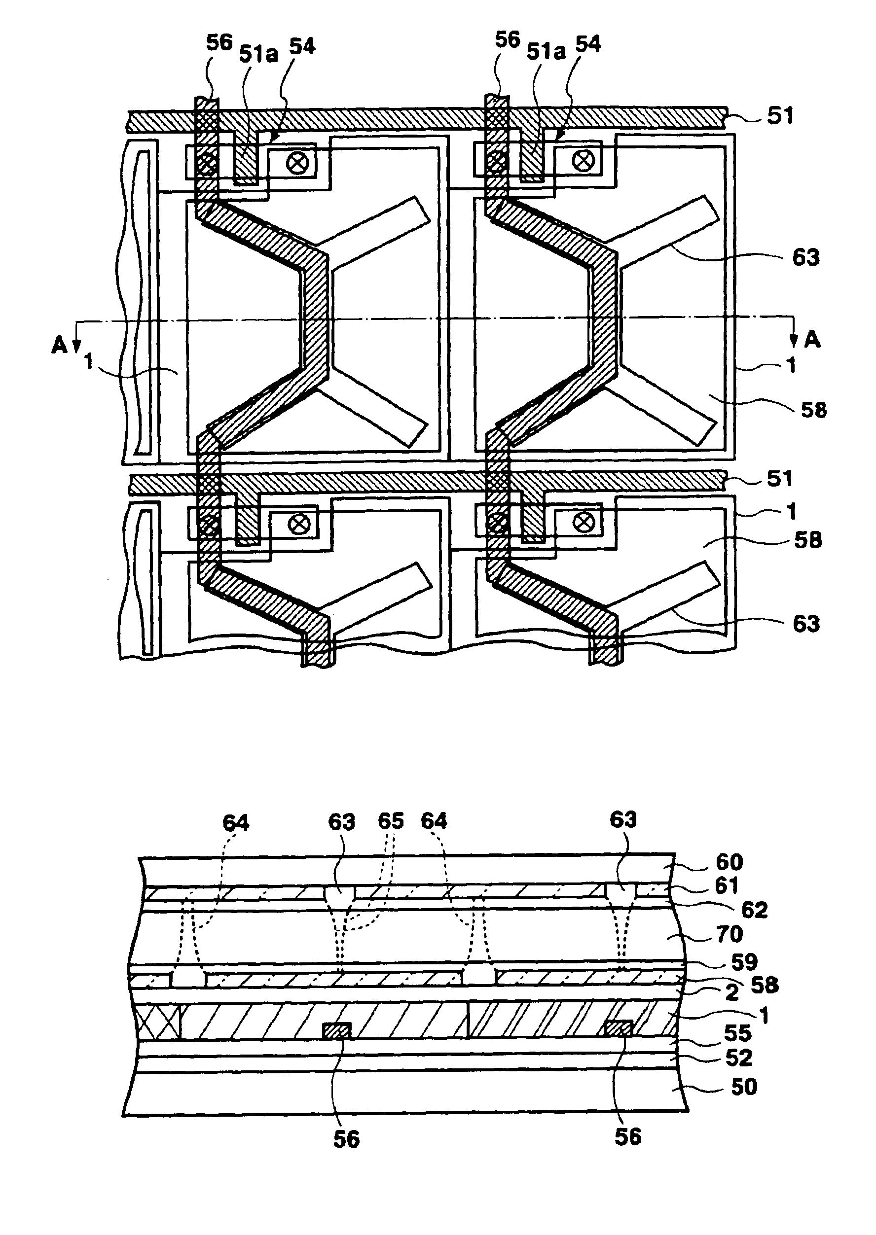
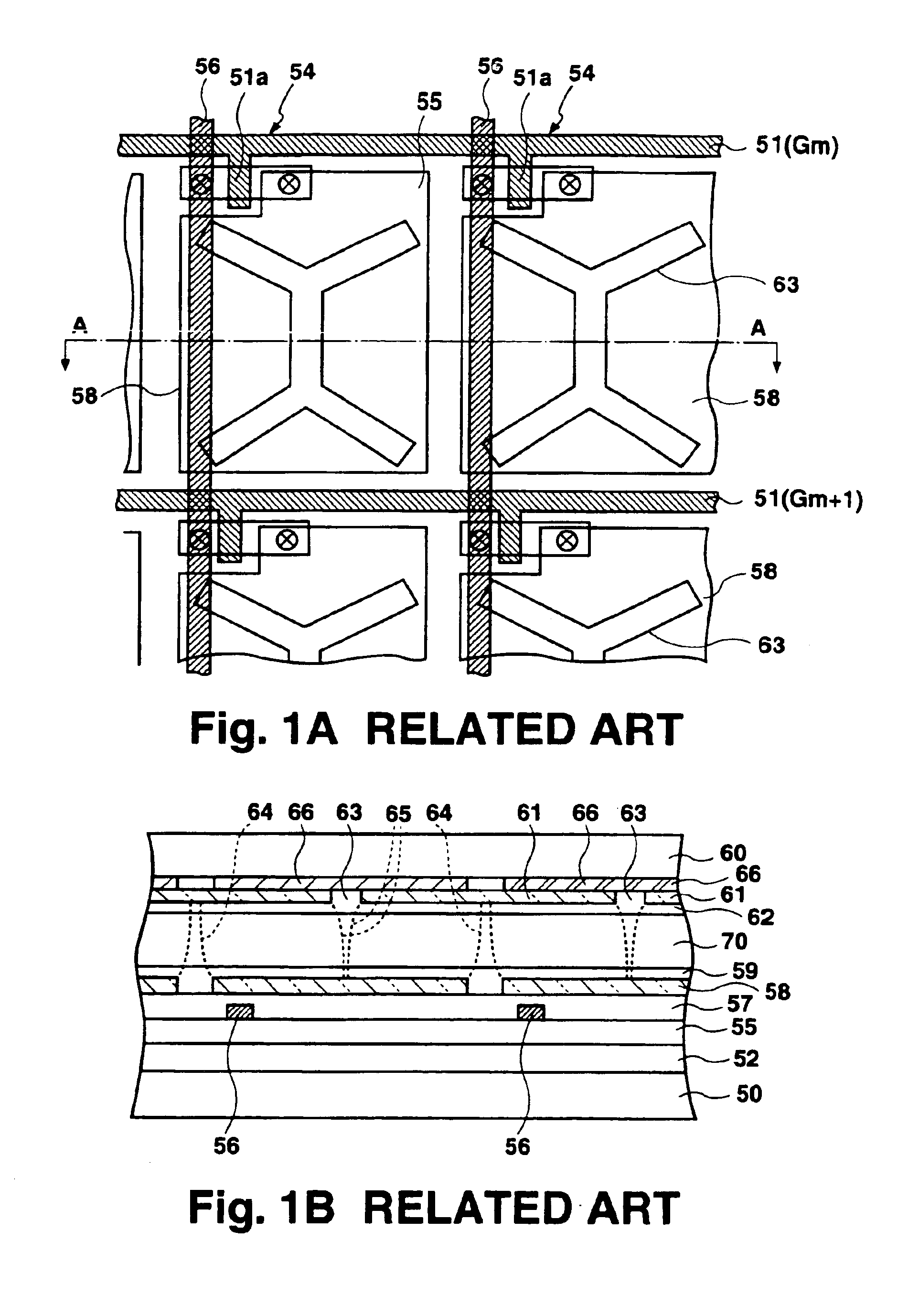
[0053]FIG. 3A is a plan view showing a first embodiment of the present invention, and FIG. 3B is a cross-sectional view of FIG. 3A. A gate line 51 having gate electrodes 51a is formed on a first substrate 50, and a gate insulating film 52 is formed covering the gate line 51. Above these, a poly-silicon film is provided in the shape of discrete islands that cross over the gate electrodes 51a. The poly-silicon film is then doped with impurities to, together with the gate electrodes 51a, form TFTs 54. An interlayer insulating film 55 is formed over these components, and a data line 56 is superimposed on the interlayer insulating film 55. Formed covering the data line 56 are color filters 1 each colored either one of red (R), green (G), and blue (B), or alternatively, cyan, magenta, and yellow. A pixel electrode 58 composed of ITO is formed over each color filter 1, with a planarizing film 2 disposed in between. Each pixel electrode 58 is connected to a TFT 54 via a contact hole opened ...


PUM

PropertyMeasurementUnit
dielectric constantaaaaaaaaaa
voltageaaaaaaaaaa
voltageaaaaaaaaaa

Abstract

In a liquid crystal display having liquid crystal sealed between first and second substrates opposing one another, the first substrate is provided with data lines (56) formed overlapping pixel electrodes (58). By forming color filters (1) in a layer between the data lines (56) and the pixel electrodes (58), the distance between the data lines (56) and the pixel electrodes (58) is increased, reducing parasitic capacitance generated therebetween. Effective voltage application to the pixel electrodes (58) is thereby accomplished, allowing increase in contrast. No decrease in transmittance is caused because the thickness of the planarizing film (2) is not increased.

Description

[0001]This is a continuation of application Ser. No. 09 / 500,114 filed Feb. 8, 2000 now U.S. Pat. No. 6,639,640, which application is hereby incorporated by reference in its entirety.BACKGROUND OF THE INVENTION[0002]1. Field of the Invention[0003]The present invention relates to a liquid crystal display (LCD), and more particularly to improving image display of a LCD in which a source line is formed overlapping pixel electrodes.[0004]2. Description of the Related Art[0005]A vertical orientation type LCD comprising liquid crystal having negative anisotropy of dielectric constant and a vertical orientation film has been proposed in, for example, JPA H06-301036. An LCD of this type is described below.[0006]FIG. 1A is a plan view showing such a LCD, and FIG. 1B shows a cross-sectional view taken along line A-A′ of FIG. 1A. A gate line 51 is formed on a first substrate 50, and a gate insulating film 52 is formed covering the gate line 51. The gate line 51 comprises gate electrodes 51a wit...

Claims


Application Information

Patent Timeline
Patent Type & Authority Patents(United States)
IPC IPC(8): G02F1/13G02F1/1333G02F1/1343G02F1/1362G09F9/30G02F1/1335G02F1/1337G02F1/135
CPCG02F1/133707G02F1/1343G02F1/136286G02F1/135
Inventor MATSUOKA, HIDEKIMAEDA, KAZUYUKIOIMA, SUSUMU
Owner SANYO ELECTRIC CO LTD
Why Eureka
Try Eureka