Wafer chuck with integrated reference sample

a reference sample and chuck technology, applied in the field of optical metrology devices, can solve the problems of increasing the complexity of the instrument and its cost and size, the prior approach of placing the reference chip outside the circular chuck and connecting the chuck to the chuck cannot be implemented in a rotational system, and achieves the effect of increasing the wafer-throughput, reducing the cost of the instrument, and improving the accuracy of the positioning of the reference chip

Inactive Publication Date: 2005-10-04
THERMA WAVE INC
View PDF5 Cites 60 Cited by
  • Summary
  • Abstract
  • Description
  • Claims
  • Application Information

AI Technical Summary

Benefits of technology

[0009]Locating the reference specimen within the area of the chuck used for wafer clamping enables an economy of design. The required range of stage-travel is set by the wafer dimensions. This admits the use of extremely short-travel translation stages to access large wafer areas. For example, the entire surface of a 300 mm diameter wafer can be accessed using a single 270 degree rotary-stage in combination with two ±75 mm linear-travel stages, e.g. ±75 mm of travel in the x direction and ±75 mm in the y direction. The economy of motion enables increased accuracy of wafer positioning and increased wafer-throughput at reduced cost.

Problems solved by technology

For systems employing z-axis rotation stages, restrictions posed by rotation symmetry, the location of auxiliary metrology instrumentation and the location and design of the wafer handling equipment make locating the reference sample more difficult.
Even when a suitable location can be identified this often requires a more expensive, long-travel stage to be used so that the reference sample can be moved to the measurement position.
These factors increase both the complexity of the instrument and its cost and size.
In particular, the prior approach of placing a reference chip outside a circular chuck and connected to the chuck cannot be implemented in a rotational system where an external pin lifter mechanism is used to raise wafer.

Method used


Image

  • Wafer chuck with integrated reference sample
  • Wafer chuck with integrated reference sample
  • Wafer chuck with integrated reference sample

Examples


Embodiment Construction

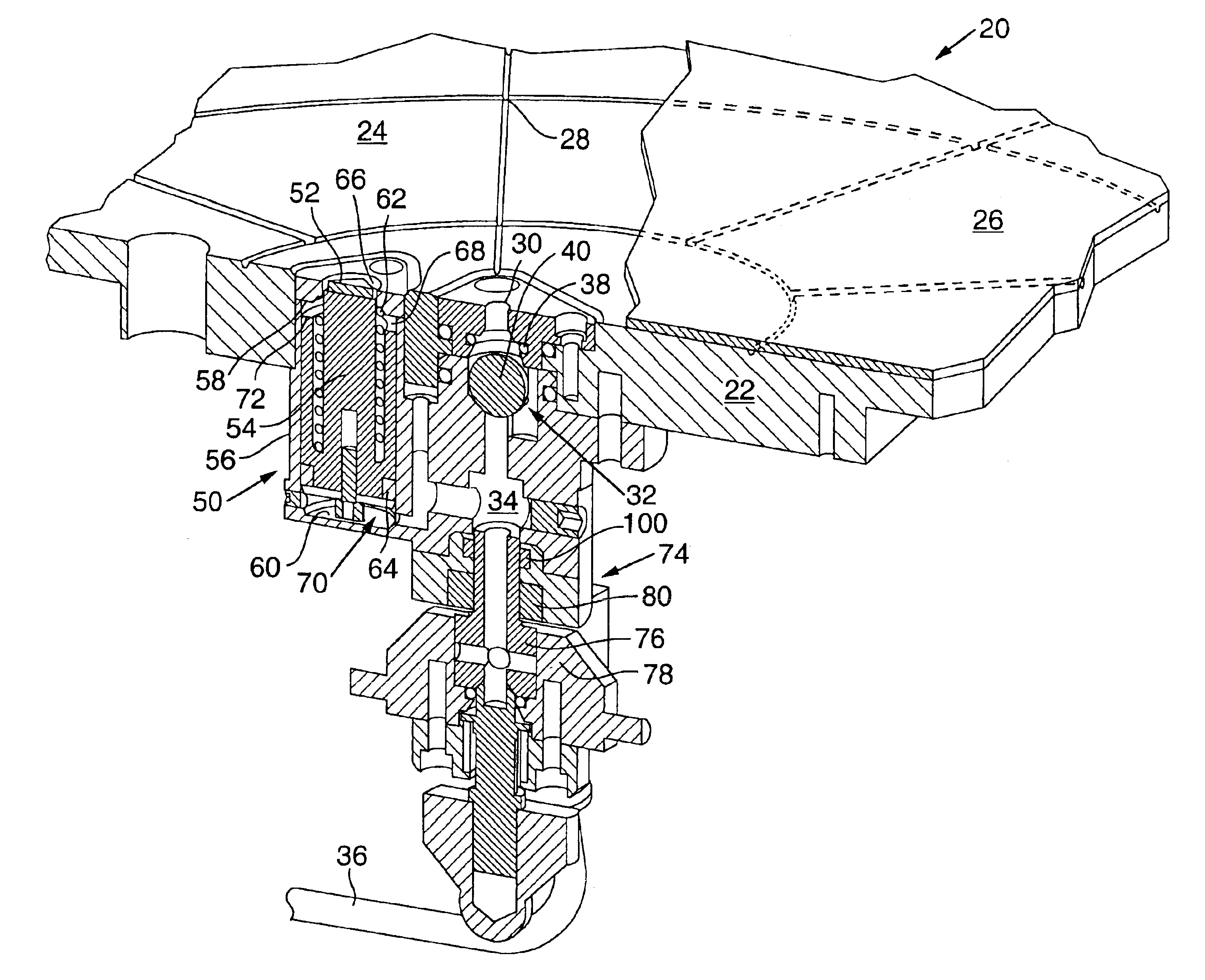
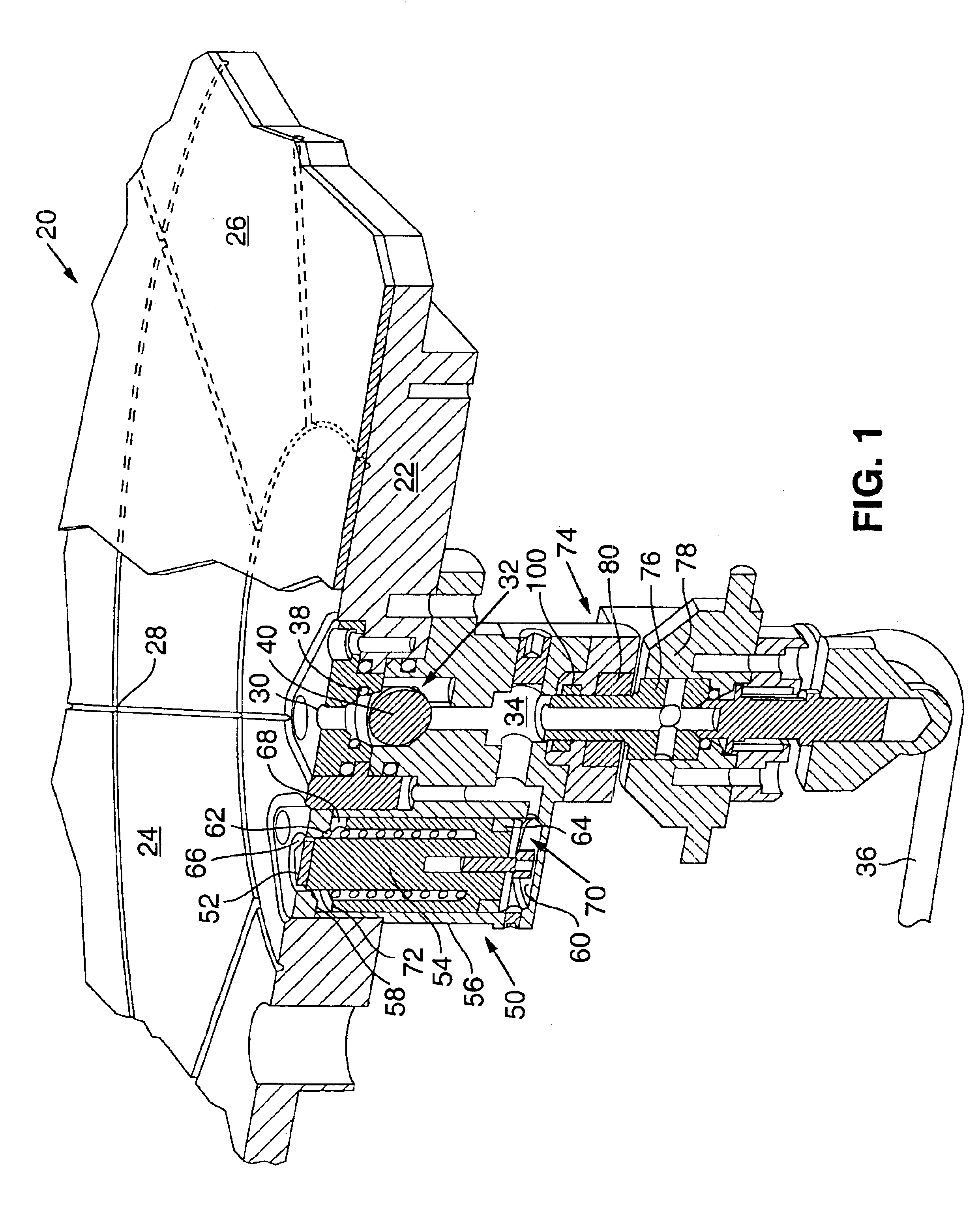
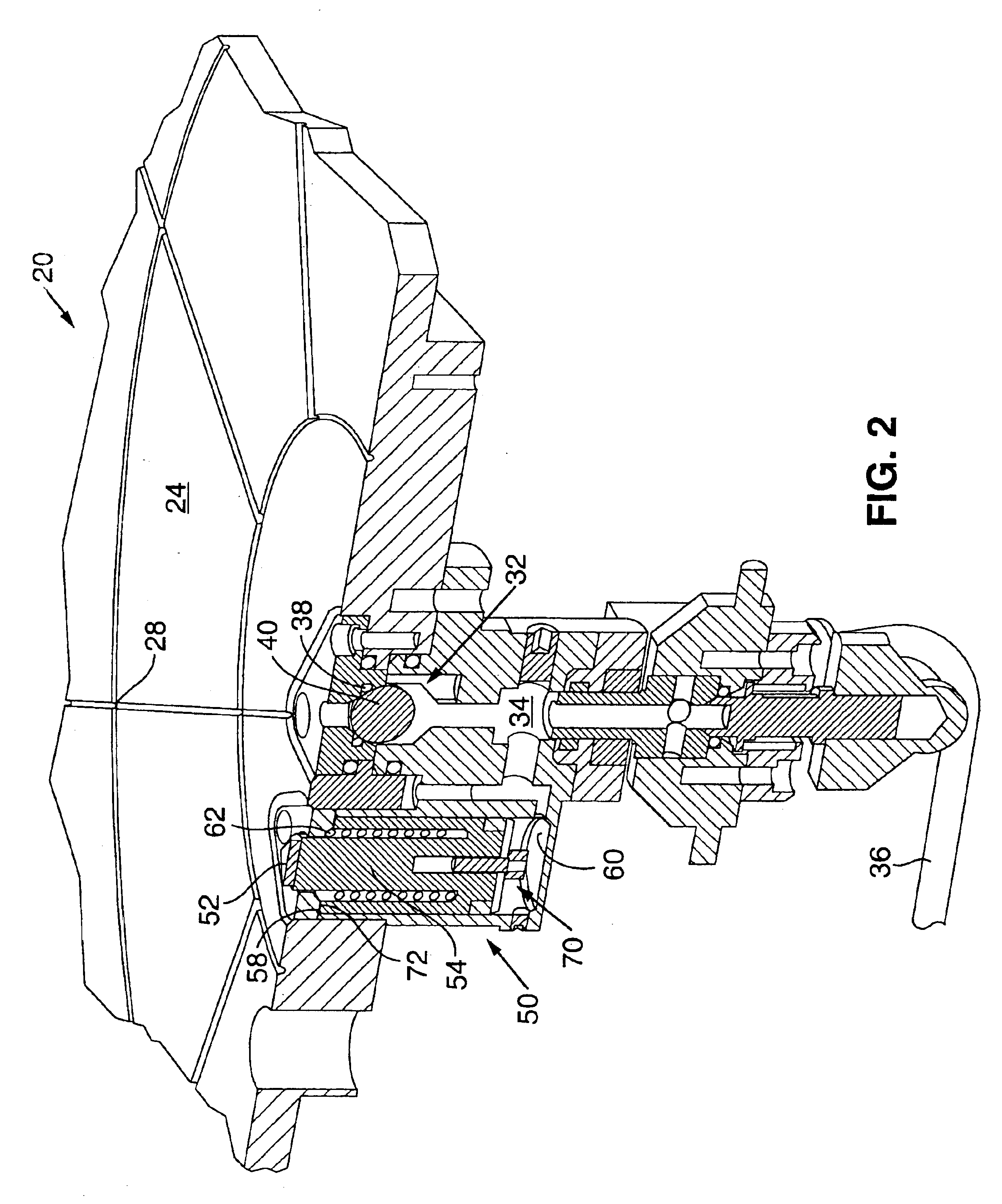
[0014]FIGS. 1 and 2 are cross-sectional schematics of a preferred embodiment of the wafer-chuck 20 showing the position of holder 50 during wafer metrology and measurement of the reference sample. FIG. 1 illustrates the configuration of the chuck employed in the metrology of wafer 26. FIG. 2 illustrates the configuration of the chuck during measurement of reference sample 52.

[0015]Wafer-chuck 20 includes a platform 22 for supporting and clamping a wafer 26. Platform 22 includes a support surface 24 for locating and supporting the wafer. The locating surface further includes a series of intersecting radial and circular channels 28 which may be connected to a vacuum supply via orifice 30, check valve assembly 32, manifold 34 and supply line 36. When supply line 36 is connected to a vacuum system, surface 22, channels 28, orifice 30, check-valve assembly 32, manifold 34 and supply line 36 comprise a vacuum wafer-chuck. In the preferred embodiment supply line 36 may be alternately conne...


PUM

PropertyMeasurementUnit
diameteraaaaaaaaaa
diameteraaaaaaaaaa
rotationaaaaaaaaaa

Abstract

The subject invention relates to a wafer stage, such as may be used in optical wafer metrology instruments. The stage contains a wafer-chuck that can be connected to translation stages for the purpose of clamping and translating the wafer so that a plurality of sites on the wafer surface may be measured. The chuck includes a holder for mounting a reference sample. The holder is movable between a retracted position where the reference sample is held below the chuck surface and an extended position, such as where the surface of the reference sample is co-planar with the wafer surface. Therefore the holder may be installed within the area of the chuck that is utilized for wafer clamping. By this arrangement, the size of the wafer translation system can be reduced minimizing the stage travel and enabling increased spatial resolution, increased wafer throughput and reduced capital equipment and operating costs.

Description

[0001]The present application is a continuation of U.S. patent application Ser. No. 10 / 050,653, filed Jan. 14, 2002, and now U.S. Pat. No. 6,757,059, which claims priority to the U.S. Provisional Patent Application Ser. No. 60 / 287,360 filed Apr. 30, 2001, and Ser. No. 60 / 336,515 filed Nov. 1, 2001, both of which are incorporated herein by reference.TECHNICAL FIELD[0002]The subject invention relates to optical metrology devices which include a movable stage for rastering a wafer with respect to a measuring probe beam. More specifically, the invention relates to a stage which includes a system for mounting a reference chip within the footprint of the wafer thereby reducing the amount of stage travel necessary to measure both the wafer and the reference chip.BACKGROUND OF THE INVENTION[0003]Optical metrology instruments require periodic monitoring and calibration. The output intensity of the light sources, the nature and extent of solarization of the optical components, chemical contam...

Claims


Application Information

Patent Timeline
Patent Type & Authority Patents(United States)
IPC IPC(8): G01N21/01H01L21/00G01N21/88G01N21/95
CPCG01N21/01H01L21/67253G01N21/9501
Inventor EBERT, MARTINTRABER, THOMAS
Owner THERMA WAVE INC
Why Eureka
Try Eureka