If the circuitry initially receives the power signals and the control signals simultaneously, damage to the circuitry will occur and the damaged circuit board assembly will require replacement.
Unfortunately, there are deficiencies to the above-identified conventional approaches to installing a circuit board assembly within an interconnection subsystem.
For example, the user may attempt to install the circuit board assembly too quickly without allowing the circuit board assembly to properly seat within the card cage.
In particular, the user may push the circuit board assembly in a rough or thrusting manner even though the circuit board is not properly nestled within its slot of the card cage.
In such a situations, the circuit board connectors will not be properly aligned with the
backplane connectors.
Thus, as the user continues to apply force on the circuit board assembly (e.g., by operating the levers), one or more components may sustain damage due to the misalignment.
Such damage is particularly likely when the circuit board assembly and / or the interconnection subsystem suffers from a buildup of worst case mechanical tolerances.
That is, since the levers of the circuit board assembly are capable of partially rotating in response to contact with the card cage, it is possible for the user to over-install the circuit board assembly into the card cage in a single, continuous motion (e.g., with a strong push) and thus not wait long enough for the power-up sequence to complete (i.e., and thus not provide enough time for the circuitry to reach a stable and controlled state before receiving signals other than the power signals).
Such a
scenario is particularly likely if the user is not well-trained or if the user is unaware of the manufacturer's requirement for installation to occur in a staggered manner.
Furthermore, even if the user is well-trained, it is still possible for the user to accidentally over insert the circuit board assembly causing the circuit board assembly to receive control signals too soon.
For example, it may be difficult for the user to judge the proper amount of force and distance to push the circuit board assembly due to tolerance differences in the circuit board assembly and / or the interconnection subsystem and move the circuit board assembly too far forward so that the power
signal pins and the
control signal pins connect concurrently.
Additionally, the user may misjudge the amount of time that passes before completing the installation and complete the installation before the power-up sequence is finished.
As a result, regardless of whether the user is well-trained or not, it is very easy for the user to install the circuit board assembly too quickly and thus damage the circuit board assembly.
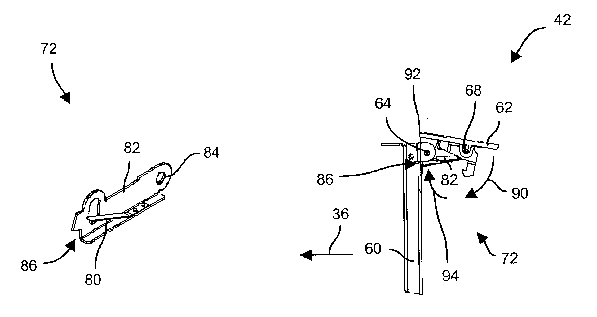
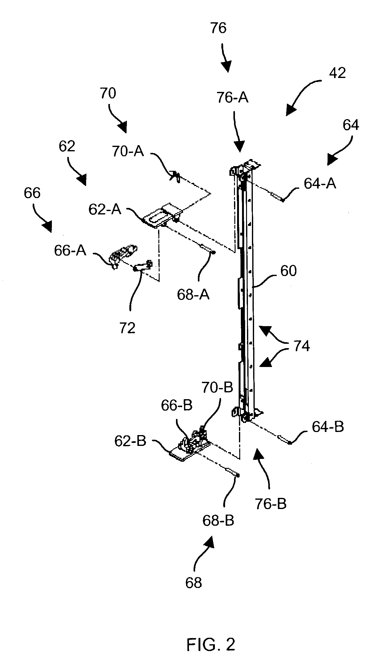
Due to the operation of the insertion delay latch, the installation process tends to be slightly slower and smoother thus providing time for connectors to properly align and, if a time delay is needed, time for a power-up sequence to complete before completing installation.

