Industrial process fault detection using principal component analysis

a technology of industrial process and principal component analysis, applied in the direction of testing/monitoring control system, instruments, nuclear elements, etc., can solve the problems of loss of at least about $75,000 in revenues, monitoring operations that do not necessarily provide an indication of how the plasma process is actually proceeding, and plasma may not be performing properly

Inactive Publication Date: 2005-10-04
PEAK SENSOR SYST
View PDF20 Cites 44 Cited by
  • Summary
  • Abstract
  • Description
  • Claims
  • Application Information

AI Technical Summary

Benefits of technology

[0009]Accordingly, one object of the present invention is to provide a more accurate indication of how an entire industrial process, such as a plasma process, has proceeded on a more “real-time” basis, and thereby allow for a reduction in the number of product units (e.g., semiconductor wafers) that are exposed to abnormal processes.

Problems solved by technology

Further consider that an eight inch wafer which is processed in one of these chambers in some cases may be used to produce up to 600 individual semiconductor chips which are each worth at least about $125, and that each of these semiconductor chips are in effect “pre-sold.” Therefore, a single wafer which has undergone an abnormal plasma process and which is scrapped can result in lost revenues of at least about $75,000.
However, no semi-conductor devices are formed from a qualification wafer as qualification wafers are processed and retained solely for testing / evaluating the plasma process, whereas semiconductor devices are formed from the production wafers.
However, these types of monitoring operations do not necessarily provide an indication of how the plasma process is actually proceeding.
All of the “hardware” settings may be correct, but still the plasma may not be performing properly for a variety of reasons (e.g., an “unhealthy” plasma).
Since errors in a plasma process are typically detected by some type of post processing, destructive testing technique, multiple wafers are typically exposed to the faulty plasma process before the error is actually identified and remedied resulting in many wafers that need to be scrapped at great cost.
As may be appreciated, such techniques can be quite computationally intensive due to the amount of spectral data involved and also require the establishment of normal spectra which may be searched for a match.

Method used


Image

  • Industrial process fault detection using principal component analysis
  • Industrial process fault detection using principal component analysis
  • Industrial process fault detection using principal component analysis

Examples


Embodiment Construction

Plasma Monitoring Assembly

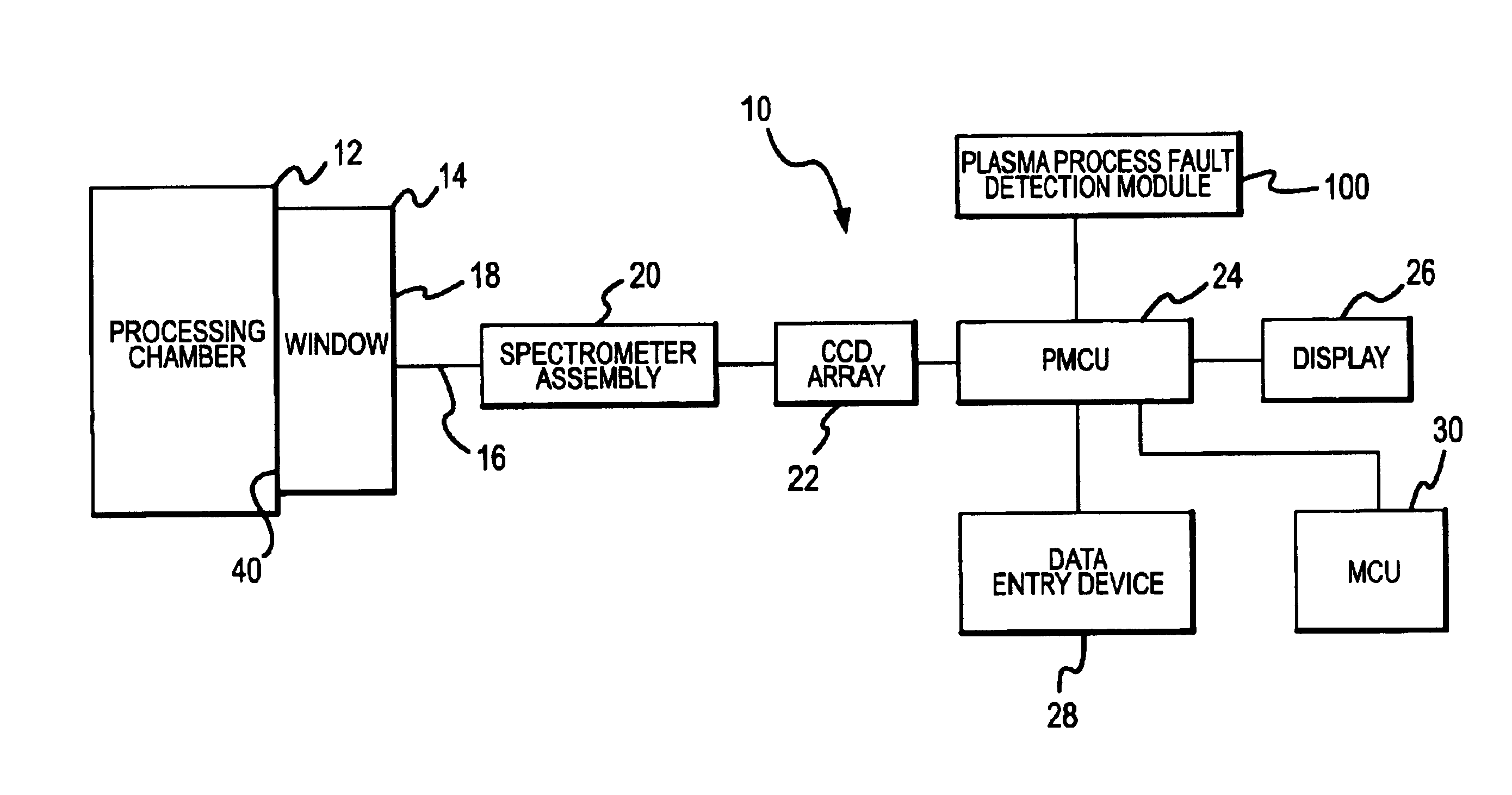
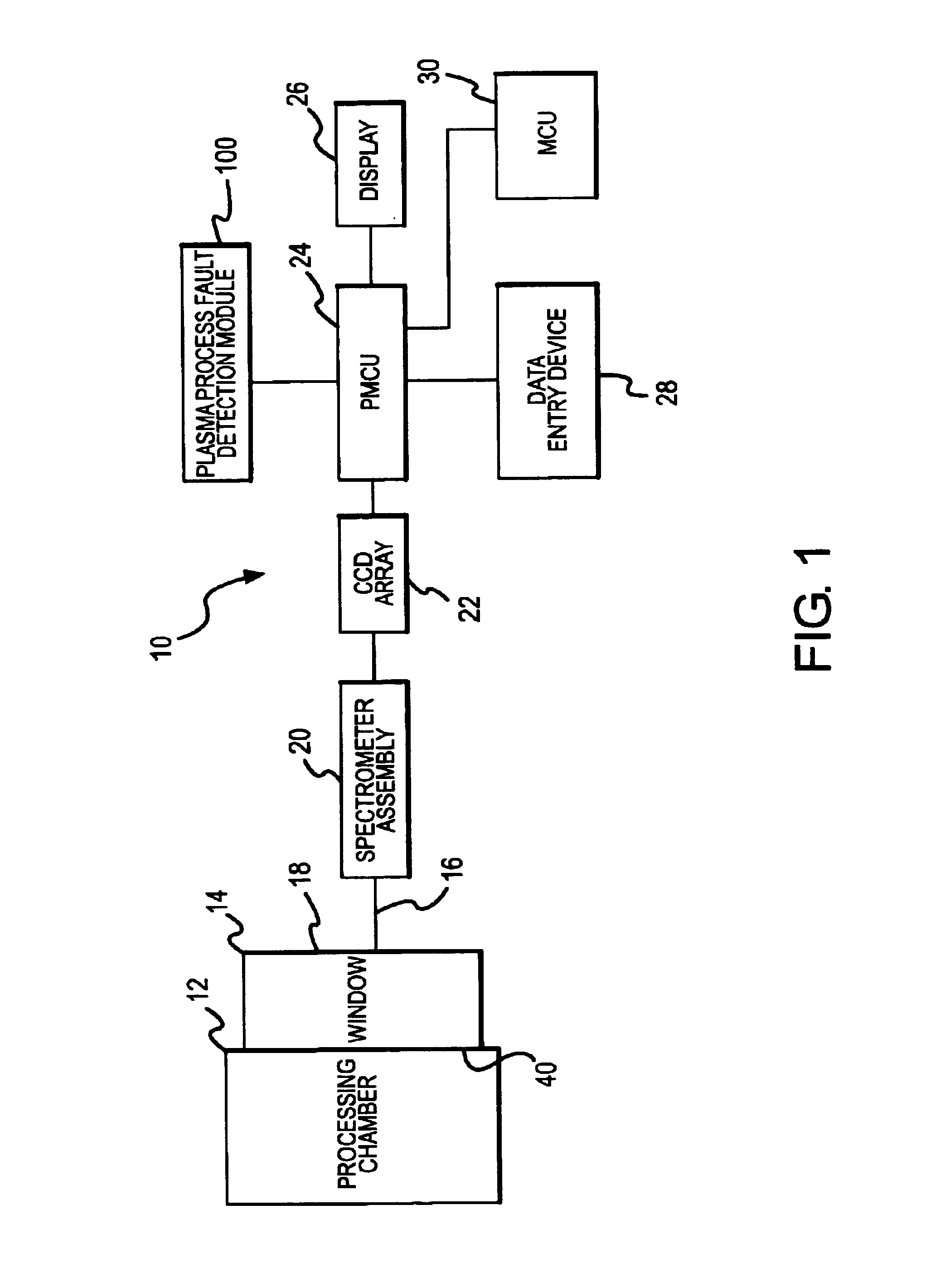
[0027]Referring to FIG. 1, there is shown one embodiment of an assembly for monitoring / evaluating plasma processes (hereafter “plasma monitoring assembly 10”) that may be used to collect optical emissions spectra (OES) data from a plasma process conducted within a plasma processing chamber 12 of a wafer production system. In other embodiments, sensors other than those of OES may be used. The plasma monitoring assembly 10 operatively interfaces with a window 14 of the plasma processing chamber 12 by receiving optical emissions of the plasma which pass out of the processing chamber 12 through the window 14. These optical emissions are “collected” by an appropriate fiber optic cable 16, one end of which is positioned at or near the outer surface 18 of the window 12. Optical emissions of the plasma within the processing chamber 12 during processing of a wafer therein enter the fiber optic cable 16 and are directed to a spectrometer assembly 20. Both scanning-ty...


PUM


Abstract

A method and system for use in monitoring / evaluating industrial processes such as, for example, plasma processes are provided. In one embodiment, a plasma process fault detection module (100) includes multiple sub-modules. A data selection sub-module (101) obtains selected optical emissions spectra (OES) data for each wafer that is processed. A model building / updating sub-module (102) constructs multiple models from the OES data for a number of wafers. A principal component analysis (PCA) analysis sub-module (103) utilizes PCA techniques to determine whether the OES data for a particular wafer differs significantly from an expected normal wafer as represented by the models. A model maintenance sub-module (104) saves and retrieves models for different processes, associating the current wafer with the correct process. A wafer categorization sub-module (105) categorizes each wafer based on a scalar metric characterizing the residual spectrum vector. A data output sub-module (106) outputs the results to a user.

Description

FIELD OF THE INVENTION[0001]The present invention relates generally to the field of evaluating the progress and efficacy of industrial processes by analyzing (in real time) the data streams produced by sensors that monitor the processes, and more particularly to monitoring / evaluating plasma processes useful in the fabrication of semiconductor microelectronic circuits, microelectromechanical devices, and the like.BACKGROUND OF THE INVENTION[0002]Industrial processes used for the manufacture of a wide variety of valuable goods are often automated such that the processing equipment performs without direct control of human operators. Sensors are typically utilized in such situations to measure aspects of the processing operation, either for direct feedback control, or for confirmation that processing conditions are within established norms.[0003]Plasma is used in various types of industrial processes in the semiconductor and printed wiring board industries, as well as in various other i...

Claims


Application Information

Patent Timeline
Patent Type & Authority Patents(United States)
IPC IPC(8): G06F11/30G05B23/02
CPCG05B23/0254
Inventor JAHNS, GARY L.ZHANG, YIXINPALLADINO, ANTHONY PETER
Owner PEAK SENSOR SYST
Why Eureka
Try Eureka