Integrated circuit devices including self-aligned contacts with increased alignment margin

Inactive Publication Date: 2005-10-11
SAMSUNG ELECTRONICS CO LTD
View PDF5 Cites 10 Cited by
  • Summary
  • Abstract
  • Description
  • Claims
  • Application Information

AI Technical Summary

Benefits of technology

[0011]According to certain embodiments, an interlayer insulating layer is on the substrate. The bit line structures may comprise a plurality of conductive plugs extending though the interlayer insulating layer to contact the second conductive pads. The conductive plugs may also contact the third c

Problems solved by technology

Accordingly, defects, such as poor contact filling or misalignment, may occur.
Such a conventional memory structure may have the following problems: Even though the contact pads 20a and 20b are self-aligned, it may be difficult to precisely align the openings at which the self-aligned contact pads 20a and 20b will be formed because the integration density of the memory d

Method used


Image

  • Integrated circuit devices including self-aligned contacts with increased alignment margin
  • Integrated circuit devices including self-aligned contacts with increased alignment margin
  • Integrated circuit devices including self-aligned contacts with increased alignment margin

Examples


Embodiment Construction

[0026]The present invention will now be described more fully with reference to the accompanying drawings, in which preferred embodiments of the invention are shown. This invention may, however, be embodied in many different forms and should not be construed as being limited to the embodiments set forth herein. Rather, these embodiments are provided so that this disclosure will be thorough and complete, and will fully convey the concept of the invention to those skilled in the art. In the drawings, the thickness of layers and regions are exaggerated for clarity. It will also be understood that when a layer is referred to as being “on” another layer or substrate, it can be directly on the other layer or substrate, or intervening layers may also be present.

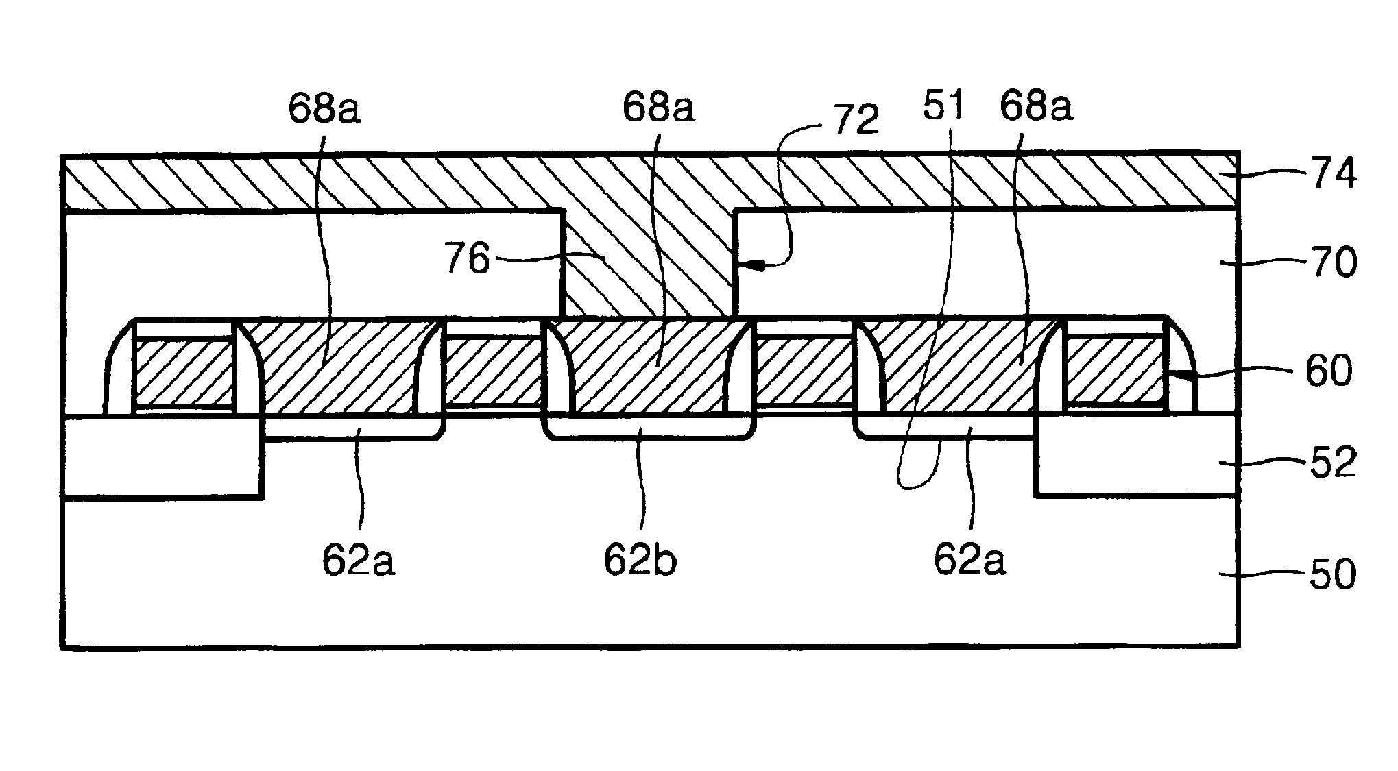
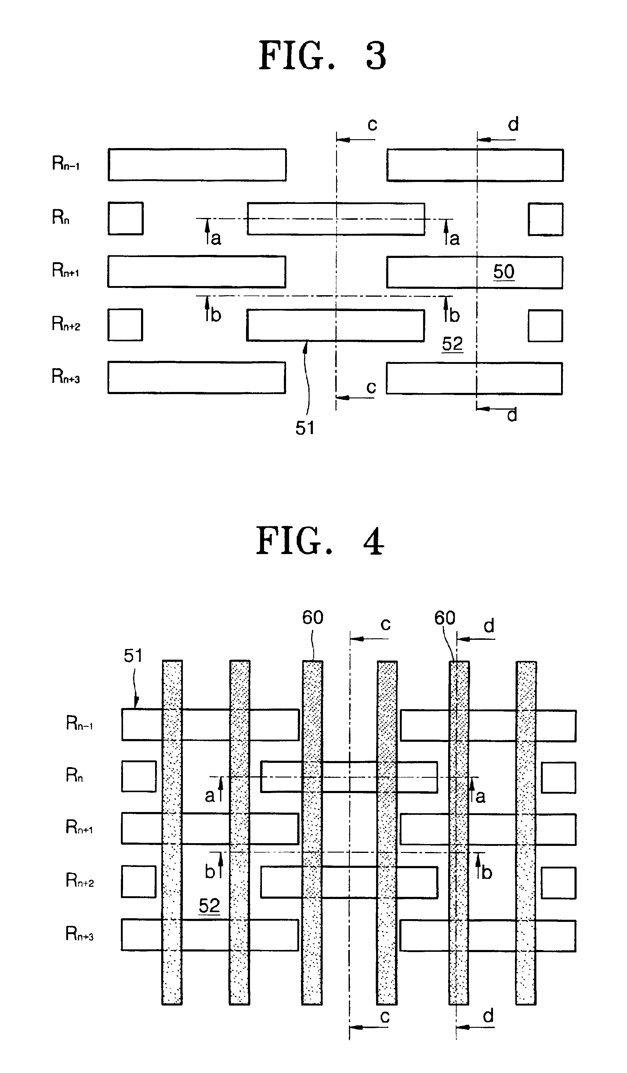
[0027]Referring to FIGS. 3 and 9A through 9D, a semiconductor substrate 50 is prepared. The semiconductor substrate 50 may be, for example, a silicon substrate including p-type or n-type impurities. A well region (not shown) is forme...


PUM


Abstract

An integrated circuit device, e.g., a memory device, includes a substrate, and a plurality of rows of active regions in the substrate, the active regions arranged in a staggered pattern such that active regions of a first row are aligned with portions of an isolation region separating active regions of an adjacent second row. Source and drain regions are in the active regions and are arranged such that each active region comprises a drain region disposed between two source regions. A plurality of word line structures are on the substrate, arranged transverse to the rows of active regions such that that word line structures cross the active regions between the source regions and the drain regions. Respective rows of conductive pads are disposed between respective adjacent word lines structures, including first conductive pads on the source regions, second conductive pads on the drain regions, and third conductive on isolation regions separating active regions. A plurality of bit line structures are on the substrate, extending transverse to the word line structures and contacting the second conductive pads. Related methods of fabrication are also described.

Description

RELATED APPLICATION[0001]This application claims priority to Korean Patent Application No. 2001-29731, filed on May 29, 2001, the contents of which are herein incorporated by reference in their entirety.FIELD OF THE INVENTION[0002]The present invention relates to integrated circuit devices and methods for fabricating the same, and more particularly, to integrated circuit devices, such as integrated circuit memory devices, with self-aligned contact (SAC) pads and methods of fabricating the same.[0003]As memory devices are designed to operate at higher speeds and to have a larger storage capacity, the integration density of integrated circuit memory devices has generally increased. For example, as the integration density of dynamic random access memories (DRAMs) has increased to more than a gigabyte, the design rule has decreased below 0.18 μm. Horizontal gaps between individual devices, vertical gaps between layers, and misalignment margins have typically been reduced in proportion t...

Claims


Application Information

Patent Timeline
IPC IPC(8): H01L21/60H01L21/02H01L21/768H01L21/8234H01L21/8242H01L27/088H01L27/108
CPCH01L21/76897H10B12/00
Inventor YANG, WON-SUKKIM, KI-NAM
Owner SAMSUNG ELECTRONICS CO LTD
Why Eureka
Try Eureka