Method of manufacturing non-volatile read only memory
a non-volatile, read only technology, applied in the direction of digital storage, instruments, semiconductor devices, etc., can solve the problems of long turn around time (tat), long tat, and the inability to create source and drain diffusion areas in a common, and achieve the effect of easy refinemen
- Summary
- Abstract
- Description
- Claims
- Application Information
AI Technical Summary
Benefits of technology
Problems solved by technology
Method used
Image

Examples
first embodiment
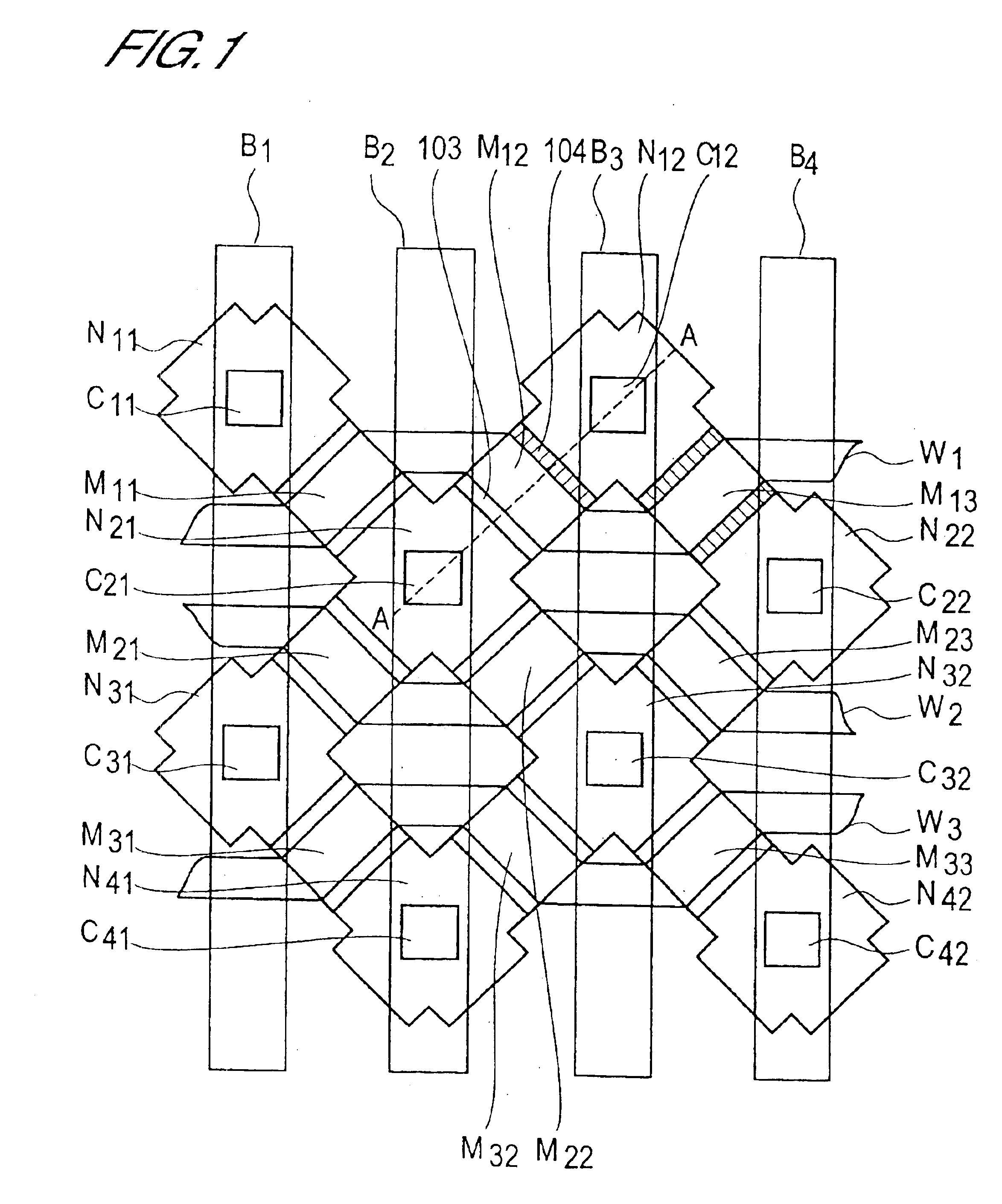
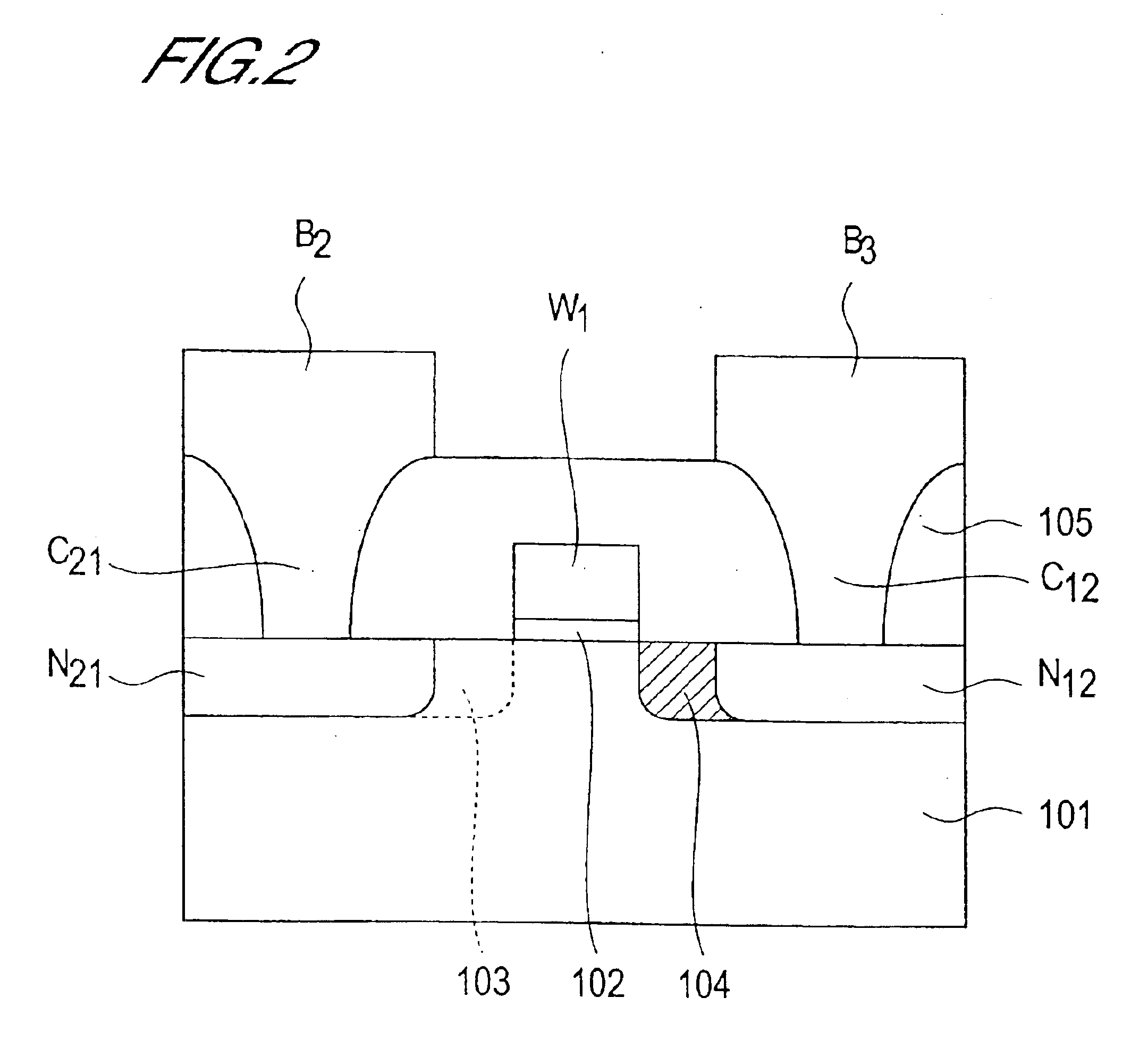
[0040]A first aspect of the embodiment of the present invention where the present invention is applied in mask ROM, will be explained using FIGS. 1 through 3.
[0041]FIG. 1 is a plan view of the structure of mask ROM relating to this aspect of the embodiment. FIG. 2 is a cross-section at A—A in FIG. 1. FIG. 3 is a circuit diagram showing the configuration of mask ROM relating to this aspect of the embodiment
[0042]n+ diffusion areas N11 through Nmn (only N11 through N42 are shown in FIG. 1) are formed on semiconductor substrate 101. As shown in FIG. 1, these n+ diffusion areas N11 through Nmn are arranged in the shape of the letter X. These n+ diffusion areas N11 through Nmn function as MOS transistor sources or drains
[0043]n+ diffusion areas N11 through Nmn are each opposite four adjoining n+ diffusion areas, thus creating memory cell MOS transistors M11 through Mpq (only M11 through M33 are shown in FIGS. 1 and 3). For example, n+ diffusion area N21 in FIG. 1 is opposite N11, N12, N3...
second embodiment
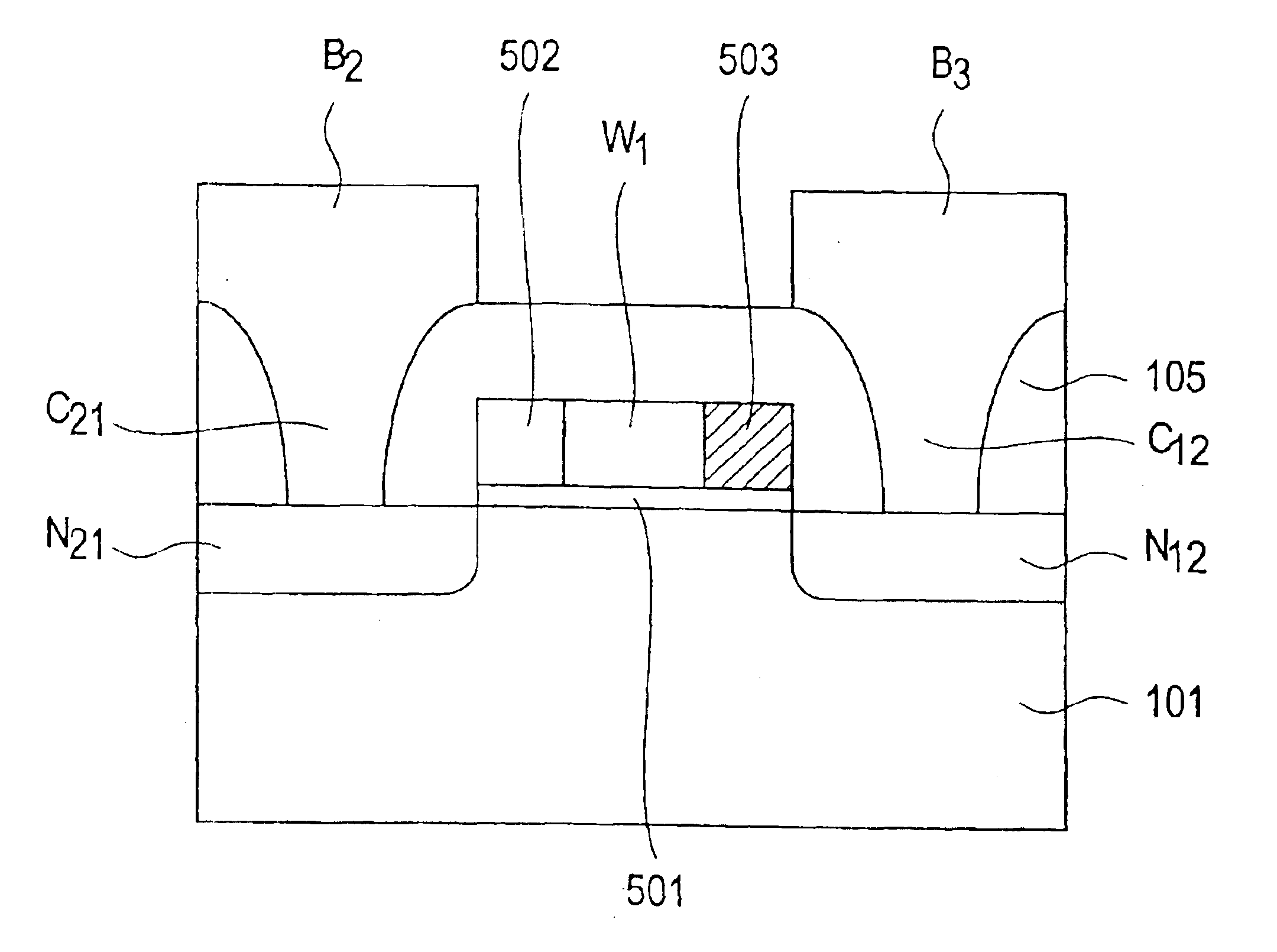
[0064]A second aspect of the embodiment of the present invention, in which the present invention is applied in mask ROM, will be explained using FIGS. 4 and 5.
[0065]The circuit configuration for the mask ROM of this aspect of the embodiment is the same as for the first aspect of the embodiment (see FIG. 3) and so explanation of it will be omitted here.
[0066]FIG. 4 is a plan view of the structure of mask ROM relating to this aspect of the embodiment. FIG. 5 is a cross-section at B—B on FIG. 4. In FIGS. 4 and 5, structural elements with the same codes as in FIGS. 1 and 2 are the same as those elements in FIGS. 1 and 2.
[0067]As shown in FIGS. 4 and 5, in the memory cell transistors used in this aspect of the embodiment, an gate oxide film 501 is formed over the entire surface of the non-diffusion area provided between the two n+ diffusion areas. Word lines W1 through Wm are formed so that they pass through the central section of this gate oxide film 501 and data write layers 502 and 50...
third embodiment
[0082]A third aspect of the embodiment of the present invention, in which the present invention is applied in mask ROM, will be explained using FIGS. 6 and 7.
[0083]The circuit configuration for the mask ROM of this aspect of the embodiment is the same as for the first aspect of the embodiment (see FIG. 3) and so explanation of it will be omitted here.
[0084]FIG. 6 is a plan view of the structure of a mask ROM relating to this aspect of the embodiment. FIG. 7 is a cross-section at C—C in FIG. 6. In FIGS. 6 and 7, structural elements with the same codes as in FIGS. 1 and 2 are the same as those elements in FIGS. 1 and 2.
[0085]As shown in FIGS. 6 and 7, in the memory cell transistors used in this aspect of the embodiment, an gate oxide film 701 is formed over the entire surface of the non-diffusion area provided between the two n+ diffusion areas. Word lines W1 through Wm are also formed so that they pass through the central section of this gate oxide film 701. Gaps 702 of at least the ...
PUM
 Abstract
Description
Claims
Application Information
 - R&D Engineer
- R&D Manager
- IP Professional
- Industry Leading Data Capabilities
- Powerful AI technology
- Patent DNA Extraction
Browse by: Latest US Patents, China's latest patents, Technical Efficacy Thesaurus, Application Domain, Technology Topic.
© 2024 PatSnap. All rights reserved.Legal|Privacy policy|Modern Slavery Act Transparency Statement|Sitemap