
Magnetic memory element and memory device including same

a technology of magnetic memory element and memory device, which is applied in the direction of digital storage, semiconductor devices, instruments, etc., can solve the problems of limited down size scaling and errors in reading stored data

Inactive Publication Date: 2005-10-18
CARNEGIE MELLON UNIV
View PDF27 Cites 63 Cited by
  • Summary
  • Abstract
  • Description
  • Claims
  • Application Information

AI Technical Summary

Benefits of technology

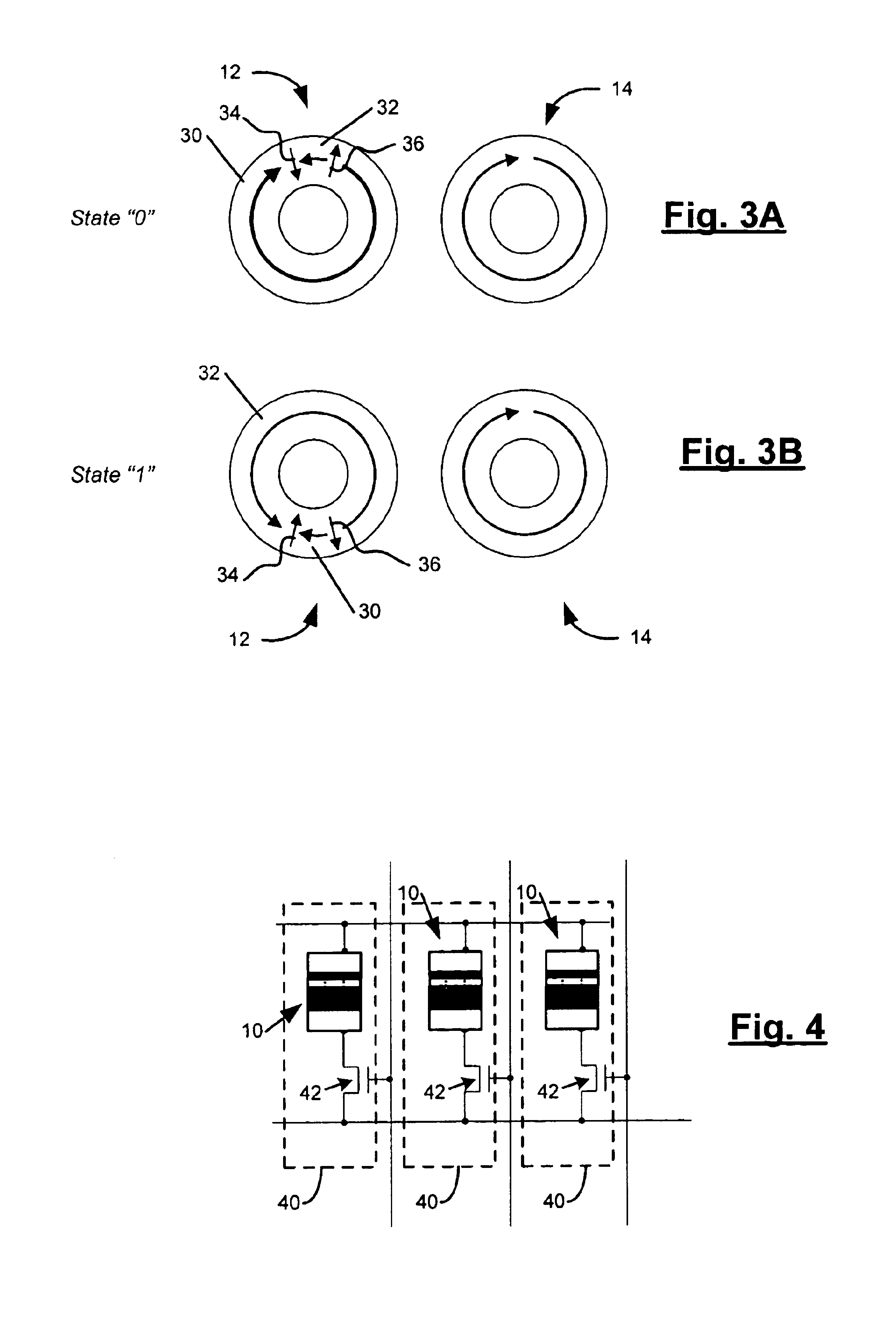
[0007]A memory cell utilizing the magnetic memory element of the present invention may provide the powerful advantage of low power operation. This is because the magnetic switching between the two binary states may be realized with very low, but circular magnetic fields. In addition, the switching current required to transition between memory states is much lower than the conventional MRAM design. Accordingly, the power consumption with a memory device according to various embodiments of the present invention may be 1000 to 10,000 times less than that of the conventional MRAM design. Moreover, various embodiments of the memory cell of the present invention require only one transistor for both read and write operations. In addition, embodiments of the memory cell eliminate the need for word lines as in conventional MRAM designs, which thereby eliminates the problem of half-selected elements, making it free of addressing disturbances. These and other benefits of the invention will be apparent from the description to follow.

Problems solved by technology

These other elements are sometimes referred to as the so-called “half-select” elements, and this is not a desirable condition because it may lead to errors in reading the stored data as well as practical limitations in down size scaling.

Method used


Image

  • Magnetic memory element and memory device including same
  • Magnetic memory element and memory device including same
  • Magnetic memory element and memory device including same

Examples


Embodiment Construction

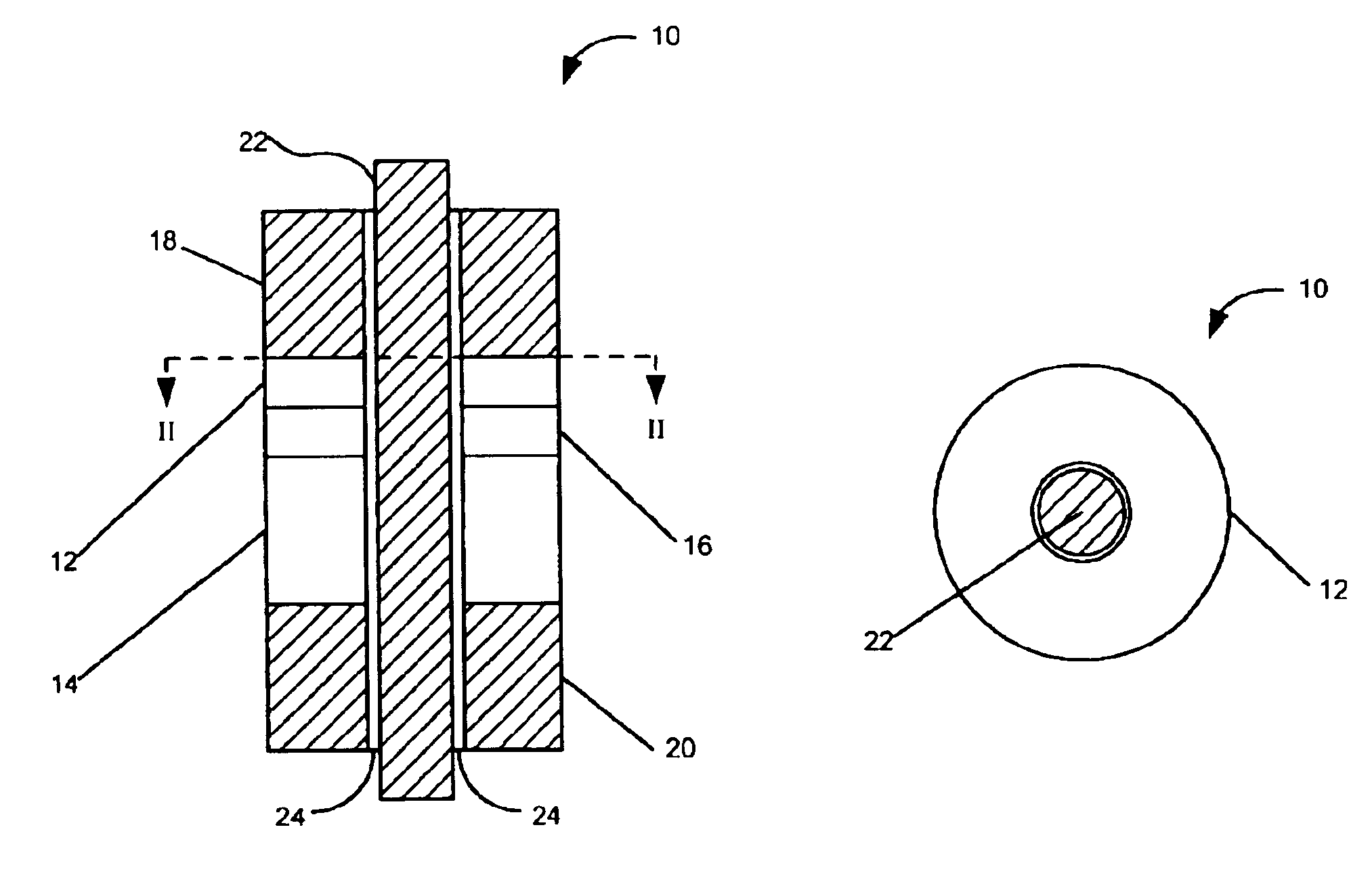
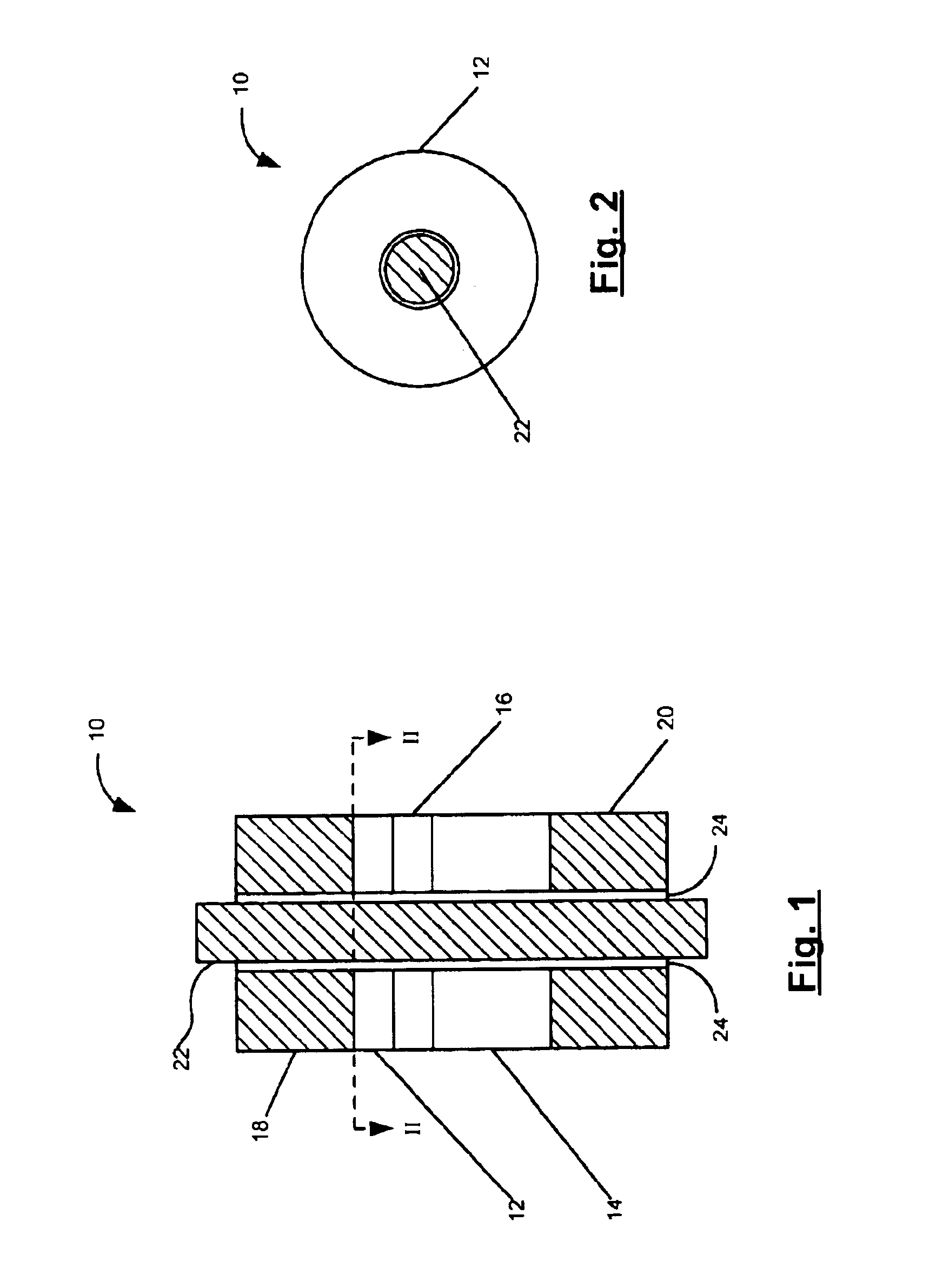
[0022]The present invention is directed, according to various embodiments, to a magnetic memory element 10, such as may be used in a magnetic memory device. FIG. 1 is a cross-sectional side view of the magnetic memory element and FIG. 2 is a cross-sectional top plan view according to various embodiments. The magnetic memory element 10 may comprise a stack of multiple closed-ended (e.g., ring-shaped) layers. The element 10 may include two magnetic layers: a storage layer 12 and a reference layer 14. The magnetic layers 12, 14 may include a magnetic material such as, for example, CoFe, NiFeCo or permalloy. The thickness of the storage layer 12 and reference layer 14 may vary depending on the materials used. For instance, the storage layer 12 may have a thickness of between, for example, 10 and 100 Angstroms and the reference layer 14 may have a thickness of, for example, greater than 100 Angstroms. The outer-to-inner diameter ratio (Dout / Din) of the magnetic memory element 10 may be, ...


PUM


Abstract

Various embodiments of a magnetic memory element, including a storage layer and a reference layer, are disclosed. The storage layer includes two conjugate magnetic domain segments having opposing helicities. The reference layer is permanently magnetized. A non-magnetic layer is interposed between the two magnetic layers. The boundaries of the two conjugate magnetic domain segments of the storage layer define domain walls along the radial direction thereof. The magnetic moment direction of one domain wall points inward and the magnetic moment direction of the other domain wall points outward. The two domain walls always attract each other, leaving one segment significantly larger than the other. These two different conditions (each longer the other) define two binary data states. By sending a vertical current through the magnetic memory element, transitions between the memory states can be achieved. Also disclosed are a memory cell, a memory device, and a computing device.

Description

CROSS-REFERENCE TO RELATED APPLICATIONS[0001]This application claims priority under 35 U.S.C. § 119 to U.S. provisional patent application Ser. No. 60 / 427,164, filed Nov. 18, 2002, which is incorporated herein by reference.STATEMENT REGARDING FEDERALLY SPONSORED RESEARCH AND DEVELOPMENT[0002]The U.S. Government may have certain Tights in any patent issued from this application as provided by Grant No. N00014-00-1-0602, awarded by the Department of Navy.BACKGROUND OF THE INVENTION[0003]Present vertical magnetic random access memory (MRAM) devices comprise a 2 D array of magnetic memory elements. The magnetic memory elements typically include many layers of magnetic and non-magnetic / electrically conductive materials. Electrical current through an associated word line is used to produce a radial magnetic field around the magnetic element to facilitate the switching (or reverse) of the magnetization of a soft (or “free”) magnetic layer of the memory element. As much as several milliAmpe...

Claims


Application Information

Patent Timeline
Patent Type & Authority Patents(United States)
IPC IPC(8): G11C11/00G11C11/16G11C11/02H01L29/66H01L29/76H01L27/22H10N50/10
CPCG11C11/16H01L27/228H01L43/08H10B61/22H10N50/10
Inventor ZHU, XIAOCHUNZHU, JIAN-GANG
Owner CARNEGIE MELLON UNIV
Learn More