Cross-point matrix for infrared touchscreen

a cross-point matrix and touchscreen technology, applied in the field of touch screen displays, can solve the problems of large border around the display area that may be undesirable, limit the styling of a unit and the ability, and increase the cost the unit as a whole, so as to reduce reduce the number of conductor traces, and reduce the effect of the size of the ring board

Inactive Publication Date: 2005-11-01
VISTEON GLOBAL TECH INC
View PDF9 Cites 22 Cited by
  • Summary
  • Abstract
  • Description
  • Claims
  • Application Information

AI Technical Summary

Benefits of technology

[0007]The present invention advantageously reduces the size of a ring board by providing a locally multiplexed, low-side driven switching matrix capable of an efficient board layout with a reduced number of conductor traces. Other advantages of reduced power supply requirements, ability to operate in high ambient light conditions, fast detection time, EMI reduction, and ESD immunity are also achieved.

Problems solved by technology

A large border around the display area may be undesirable in many applications, such as in automotive dashboard displays where space is limited.
The border also places limits on styling of a unit and the ability to put other components (e.g., mechanical control knobs or switches) close to the display area.
Furthermore, a larger size results in higher costs for the ring board and the unit as a whole.

Method used


Image

  • Cross-point matrix for infrared touchscreen
  • Cross-point matrix for infrared touchscreen
  • Cross-point matrix for infrared touchscreen

Examples


Embodiment Construction

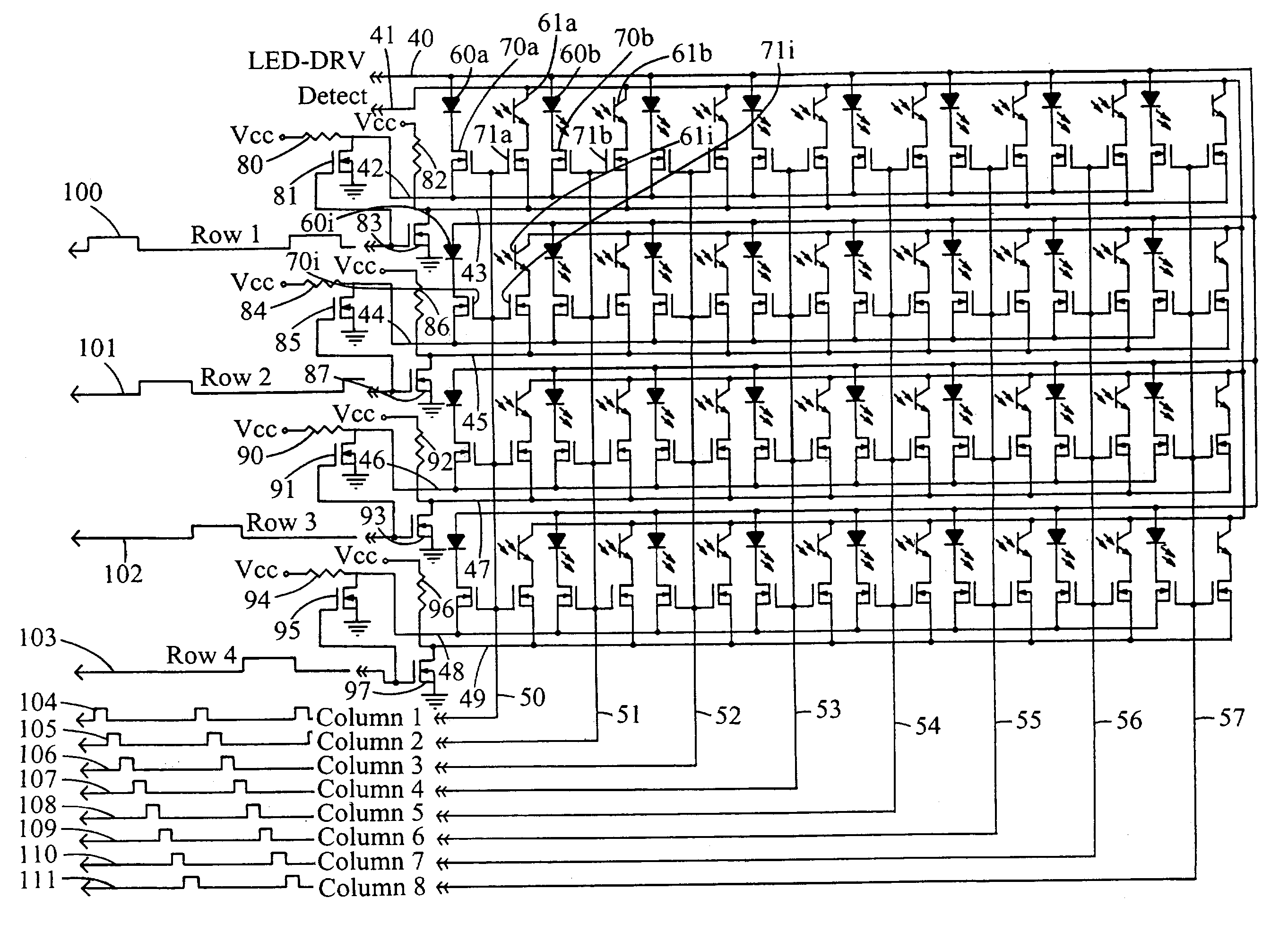
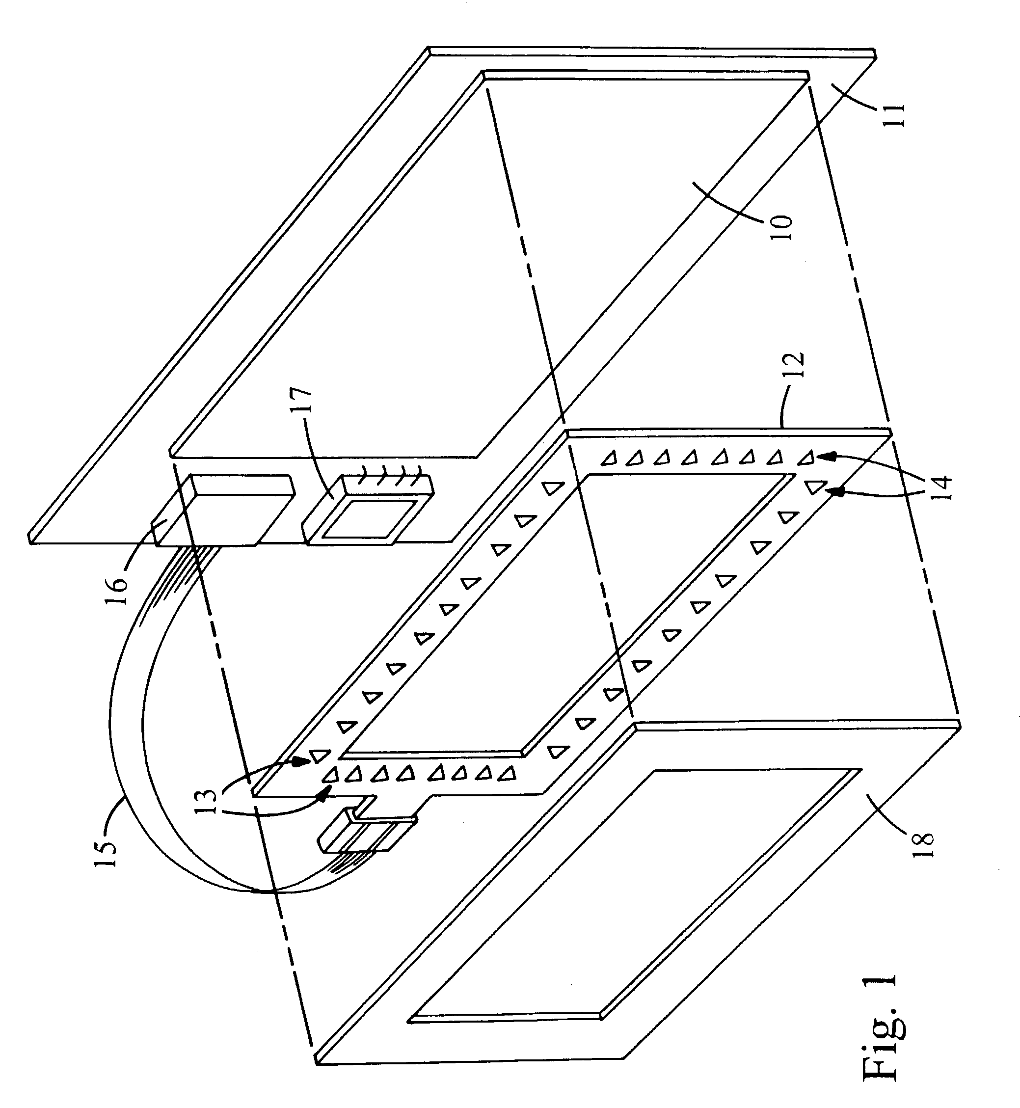
[0017]Referring to the exploded view of FIG. 1, a display panel 10 such as an active matrix liquid crystal diode (AMLCD) display is mounted to a main circuit board 11. A ring board 12 carries emitters 13 along two adjacent sides and detectors 14 along two opposite sides so that each emitter is aligned with a detector in respective pairs. In a motor vehicle application, it is preferable that the emitters be located along the bottom and left-hand edges and the detectors be located along the top and right-hand edges to minimize interference from ambient light (less light is directed upward and the driver helps block light directed toward the right-hand edge). Emitters 13 and detectors 14 can alternatively be located on the back side of ring board 12 (i.e., on the side facing display panel 10) in order to obtain additional shading from ambient light.

[0018]A wire bundle or cable 15 connects the devices on ring board 12 to control electronics 17 on main board 11 via a connector 16. A flat...


PUM


Abstract

A circuit assembly detects a touch point within a display area. A plurality of light emitters are disposed around a periphery of the display area. A plurality of detectors are disposed around the periphery, each detector being opposed to a respective light emitter. Switching circuitry for connecting the light emitters and detectors in a switching matrix has a plurality of matrix rows and matrix columns. The switching circuitry includes a plurality of row lines, each row line corresponding to a respective matrix row and a plurality of column lines, each column line corresponding to a respective matrix column. Low-side switching transistors selectably couple the light emitters and detectors to the row and column lines, respectively. A common modulated signal is coupled to the anodes of all the light emitters. A detection signal is provided by connecting the collector terminals for the detector phototransistors in common. Consequently, high-side multiplexing circuits are avoided.

Description

CROSS REFERENCE TO RELATED APPLICATIONS[0001]Not Applicable.STATEMENT REGARDING FEDERALLY SPONSORED RESEARCH[0002]Not Applicable.BACKGROUND OF THE INVENTION[0003]The present invention relates in general to touch screen displays, and, more specifically, to touch screens employing a cross-point matrix with paired light emitters / detectors disposed around the periphery of a display area which are scanned in order to detect blockage by a finger, stylus, or other pointing device pressed against the touch screen display.[0004]Infrared (IR) touch screens are widely used to correlate finger touches on a display screen by a user with soft buttons or soft keys displayed at various locations on the display screen. Typically, a number of IR emitters (i.e., transmitters) and detectors (i.e., receivers) are arranged around the periphery of the display screen to create a plurality of intersecting light paths. When the user touches the display, his or her finger blocks the IR transmission of certain...

Claims


Application Information

Patent Timeline
Patent Type & Authority Patents(United States)
IPC IPC(8): G06F3/033G06F3/042G06F3/041H01L31/10
CPCG06F3/0421
Inventor WEINDORF, PAUL FREDRICK LUTHERANDERSON, DAVID RYANMILNE, GREGORY J.
Owner VISTEON GLOBAL TECH INC
Why Eureka
Try Eureka