Real-time in-line testing of semiconductor wafers

a real-time in-line testing and semiconductor technology, applied in the testing/measurement of individual semiconductor devices, semiconductor/solid-state devices, instruments, etc., can solve the problems of incompleteness of individual operations, severe financial losses to the integrated circuit manufacturer, and large cost of ic fabrication

Inactive Publication Date: 2005-11-22
SEMILAB SEMICON PHYSICS LAB
View PDF50 Cites 3 Cited by
  • Summary
  • Abstract
  • Description
  • Claims
  • Application Information

AI Technical Summary

Problems solved by technology

Frequently, failure of an individual operation is detected only after the completion of the entire, very expensive, process of IC fabrication.
Due to the very high cost of advanced IC fabrication processes, such failures result in the severe financial losses to the integrated circuit manufacturer.
The substrate, in this procedure, does not remain in the continuous motion, so consequently the applicability of such a method for use in real-time in-line process monitoring is limited.

Method used


Image

  • Real-time in-line testing of semiconductor wafers
  • Real-time in-line testing of semiconductor wafers
  • Real-time in-line testing of semiconductor wafers

Examples


Embodiment Construction

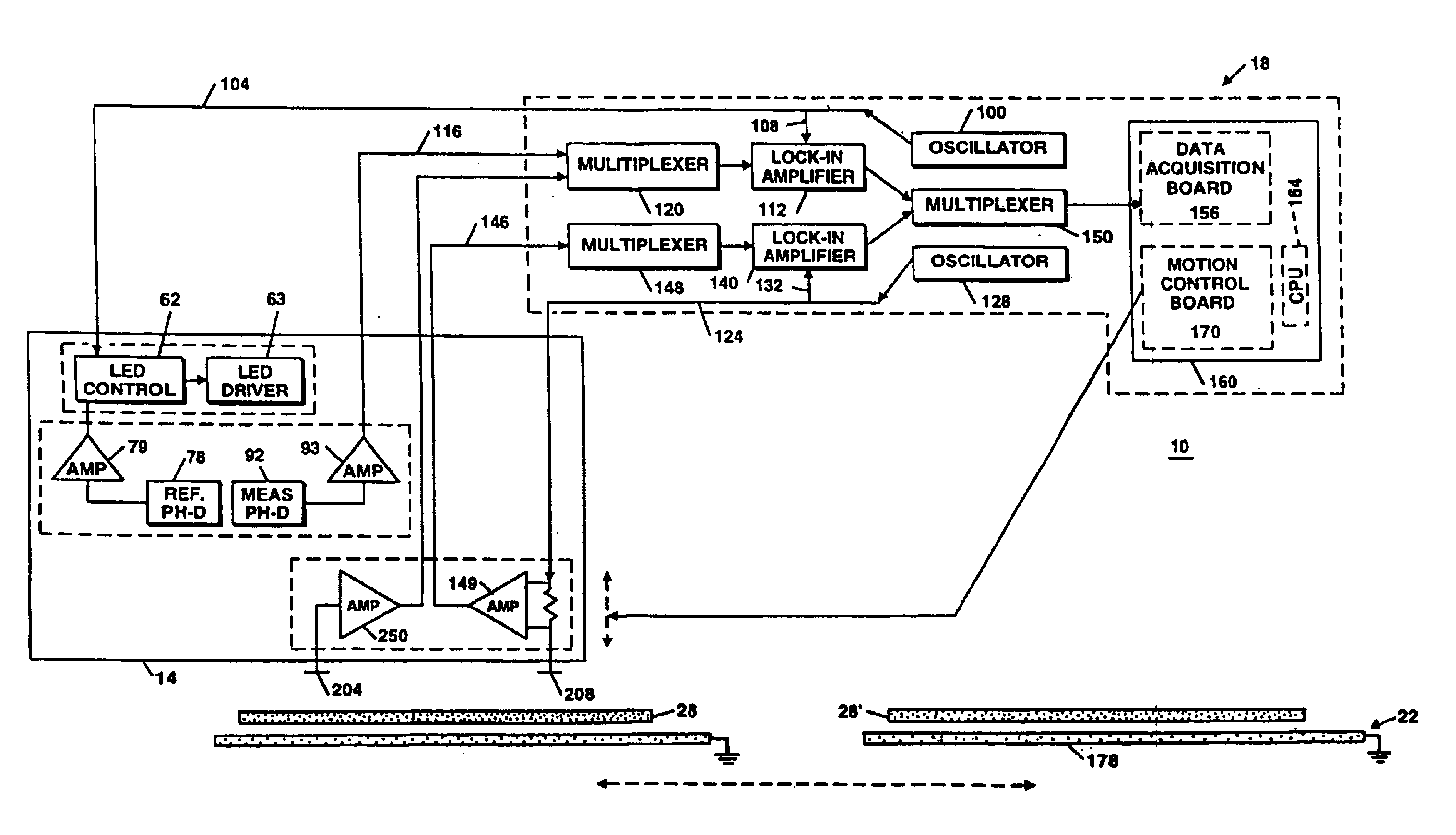
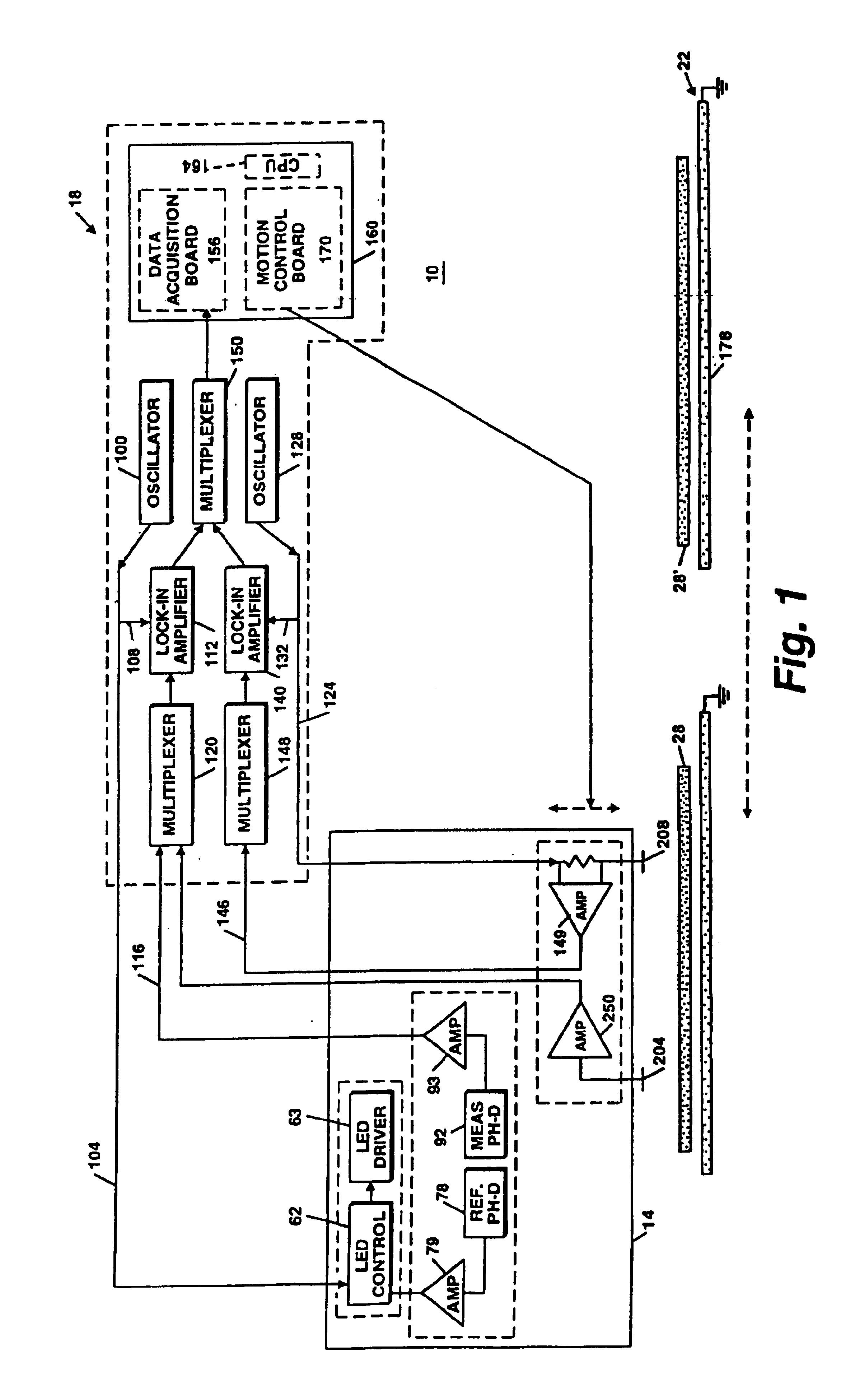
[0019]In one embodiment, the apparatus to perform various electrical characterizations makes use of the method for measuring the photo-induced voltage at the surface of semiconductor materials, termed the surface photovoltage (SPV), disclosed in the U.S. Pat. No. 4,544,887. In this method, a beam of light is directed at a region of the surface of a specimen of semiconductor material and the photo-induced change in electrical potential at the surface is measured. The wavelength of the illuminating light beam is selected to be shorter than the wavelength of light corresponding to the energy gap of the semiconductor material undergoing testing. The intensity of the light beam is modulated, with both the intensity of the light and the frequency of modulation being selected such that the resulting AC component of the induced photovoltage is directly proportional to the intensity of light and inversely proportional to the frequency of modulation.

[0020]When measured under these conditions,...


PUM


Abstract

An apparatus and method for the real-time, in-line testing of semiconductor wafers during the manufacturing process. In one embodiment the apparatus includes a probe assembly within a semiconductor wafer processing line. As each wafer passes adjacent the probe assembly, a source of modulated light, within the probe assembly, having a predetermined wavelength and frequency of modulation, impinges upon the wafer. A sensor in the probe assembly measures the surface photovoltage induced by the modulated light. A computer then uses the induced surface photovoltage to determine various electrical characteristics of the wafer.

Description

[0001]This application is a continuation of Ser. No. 09 / 932,754, filed on Aug. 17, 2001, a divisional of Ser. No. 09 / 488,647, filed on Jan. 20, 2000, now U.S. Pat. No. 6,315,574, a divisional of Ser. No. 08 / 853,171, filed on May 8, 1997, now U.S. Pat. No. 6,069,017, and a divisional of Ser. No. 08 / 396,694, filed on Mar. 1, 1995, now U.S. Pat. No. 5,661,408.FIELD OF THE INVENTION[0002]The invention relates to the testing of semiconductor wafers during manufacturing and specifically to the real-time in-line testing of semiconductor wafers during integrated circuit-fabrication.BACKGROUND OF THE INVENTION[0003]There are numerous individual operations, or processing steps, performed, in a strictly followed sequence, on the silicon wafer in the course of manufacturing a complex integrated circuit (IC). Each such operation must be precisely controlled in order to assure that the entire fabrication process yields integrated circuits displaying the required electrical characteristics.[0004]F...

Claims


Application Information

Patent Timeline
Patent Type & Authority Patents(United States)
IPC IPC(8): H01L21/66G01R31/26G01R31/265G01R31/28
CPCH01L22/14H01L2924/0002H01L2924/00G01R31/2648G01R31/2656G01R31/2831H01L22/10
Inventor KAMIENIECKI, EMILRUZYLLO, JERZY
Owner SEMILAB SEMICON PHYSICS LAB
Why Eureka
Try Eureka