Routing architecture for a programmable logic device

a programmable logic and routing architecture technology, applied in the field of integrated circuits, can solve the problems of slow circuit speed of pld, delay in the reach of transmitted signals, and inefficient routing resources on both horizontal and vertical channels,

Inactive Publication Date: 2005-11-29
ALTERA CORP
View PDF26 Cites 20 Cited by
  • Summary
  • Abstract
  • Description
  • Claims
  • Application Information

AI Technical Summary

Problems solved by technology

Maintaining the symmetrical number of pins and channel widths may cause inefficiency.
Also, if redundancy is supported such that a defective row or column of LABs is replaceable, then it would be inefficient to have the same number of routing resources (e.g., multiplexers and drivers) on both the horizontal channels and the vertical channels.
However, because the number of channels that a LAB within these architectures connect to are fewer than the L

Method used


Image

  • Routing architecture for a programmable logic device
  • Routing architecture for a programmable logic device
  • Routing architecture for a programmable logic device

Examples


Embodiment Construction

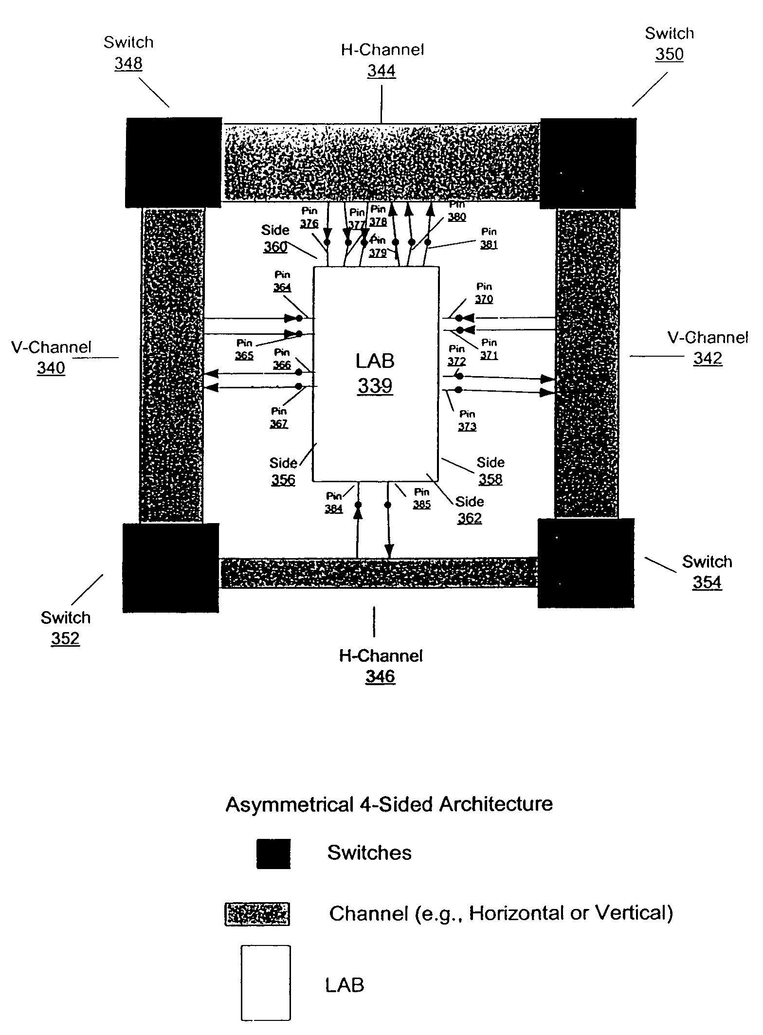
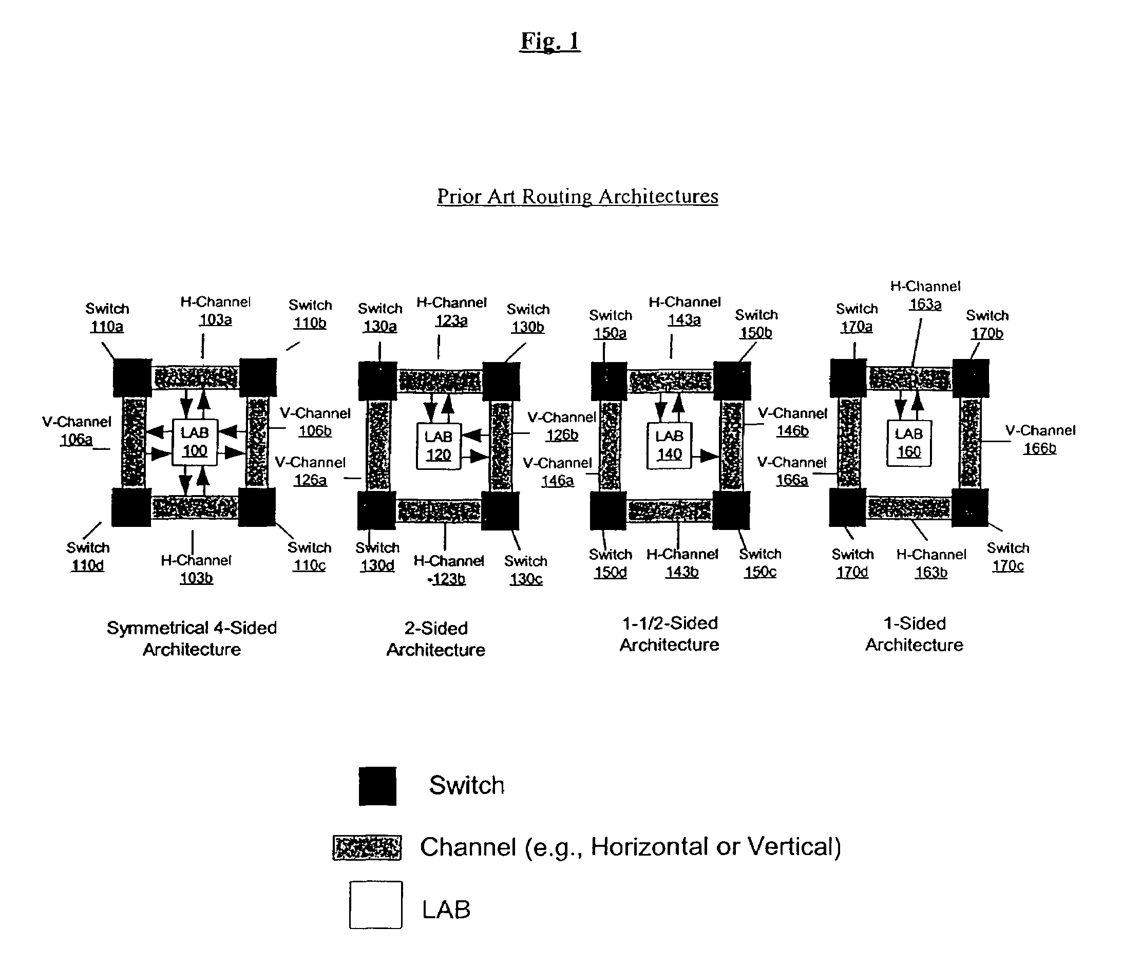
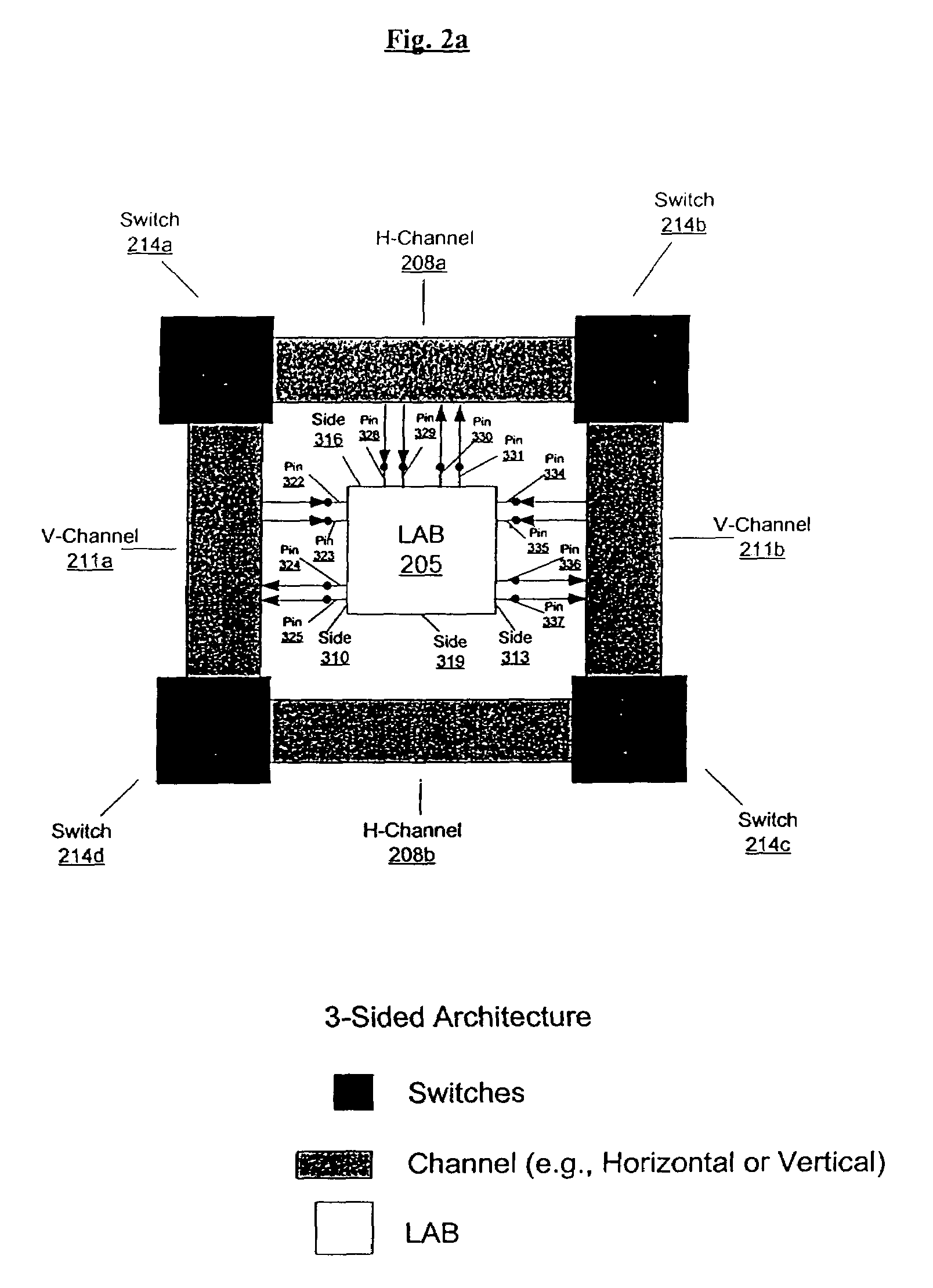
[0026]The routing architecture for the PLD provides input and output connections between a function block (e.g., the LAB, a memory block, an input / output block, an arithmetic logic unit, or a multiply-accumulate block) and horizontal and vertical channels. In one embodiment of the present invention, a function block is programmably coupled to two channels that are disposed on opposite sides of the function block (e.g., a first vertical channel disposed on the left or right side of the function block and a second vertical channel disposed on the opposite side of the function block) and another channel disposed on a third side of the function block (e.g., a horizontal channel disposed on the top side of the function block). The function block can transmit and receive signals from all three of these channels. This configuration is referred to herein as a 3-sided routing architecture.

[0027]In order to provide concrete examples, the remainder of this document refers to the 3-sided routin...


PUM


Abstract

An embodiment of this invention pertains to a 3-sided routing architecture to interconnect function blocks, such as logic array blocks (“LABs”), within a programmable logic device (“PLD”). In the 3-sided routing architecture, inputs and outputs on a first side of a function block connect to a first channel, and inputs and outputs on a second side of the function block connect to a second channel where the second side is opposite the first side. Inputs and outputs on a third side of the function block connect to a third channel. A fourth channel associated with a fourth side of the function block, the fourth side opposite the third side, is coupled only to the first channel and the second channel. In one configuration, the inputs and outputs on each of the first side, the second side, and the third side have an equal number of inputs and outputs. In this configuration, each of the first channel, the second channel, and the third channel have the same width. In another configuration, the number of pins on one of the first side, the second side, or the third side differs from the number of pins on another one of those sides.

Description

CROSS-REFERENCE TO RELATED APPLICATIONS[0001]This is a continuation application of Ser. No. 10 / 140,287 filed May 6, 2002, is now a U.S. Pat. No. 6,630,842, entitled “Routing Architecture for a Programmable Logic Device” which claims the benefit of U.S. Provisional Application Ser. No. 60 / 289,176, filed May 6, 2001.BACKGROUND OF THE INVENTION[0002]1. Field of the Invention[0003]This invention relates generally to integrated circuits and, in particular, to improved routing architectures for a programmable logic device.[0004]2. Description of the Related Art[0005]A programmable logic device (“PLD”) is a digital, user-configurable integrated circuit used to implement a custom logic function. For the purposes of this description, the term PLD encompasses any digital logic circuit configured by the end-user, and includes a programmable logic array (“PLA”), a field programmable gate array (“FPGA”), and an erasable and complex PLD. The basic building block of a PLD is a logic element that i...

Claims


Application Information

Patent Timeline
IPC IPC(8): H03K19/177
CPCH03K19/17736
Inventor LEWIS, DAVID M.LEVENTIS, PAULLEE, ANDY L.JOHNSON, BRIAN D.CLIFF, RICHARDREDDY, SRINIVAS T.LANE, CHRISTOPHER F.MCCLINTOCK, CAMERON R.BETZ, VAUGHNWYSOCKI, CHRISMARQUARDT, ALEXANDER R.
Owner ALTERA CORP
Why Eureka
Try Eureka