Providing a reference voltage to a cross point memory array

a cross-point memory and reference voltage technology, applied in the field of memory, can solve the problems of not solving many non-trivial problems and unsatisfactory layout of such devices

Inactive Publication Date: 2005-11-29
UNITY SEMICON
View PDF28 Cites 106 Cited by
  • Summary
  • Abstract
  • Description
  • Claims
  • Application Information

AI Technical Summary

Problems solved by technology

The layout of such devices are not ideal, usually requiring feature sizes of 8f2 for each memory cell, where f is the minimum feature size.
However, mere recognition that a two terminal memory element is theoretically capable of being placed in a cross point array does not solve many of the non-trivial problems associated with actually creating such a device.

Method used


Image

  • Providing a reference voltage to a cross point memory array
  • Providing a reference voltage to a cross point memory array
  • Providing a reference voltage to a cross point memory array

Examples


Embodiment Construction

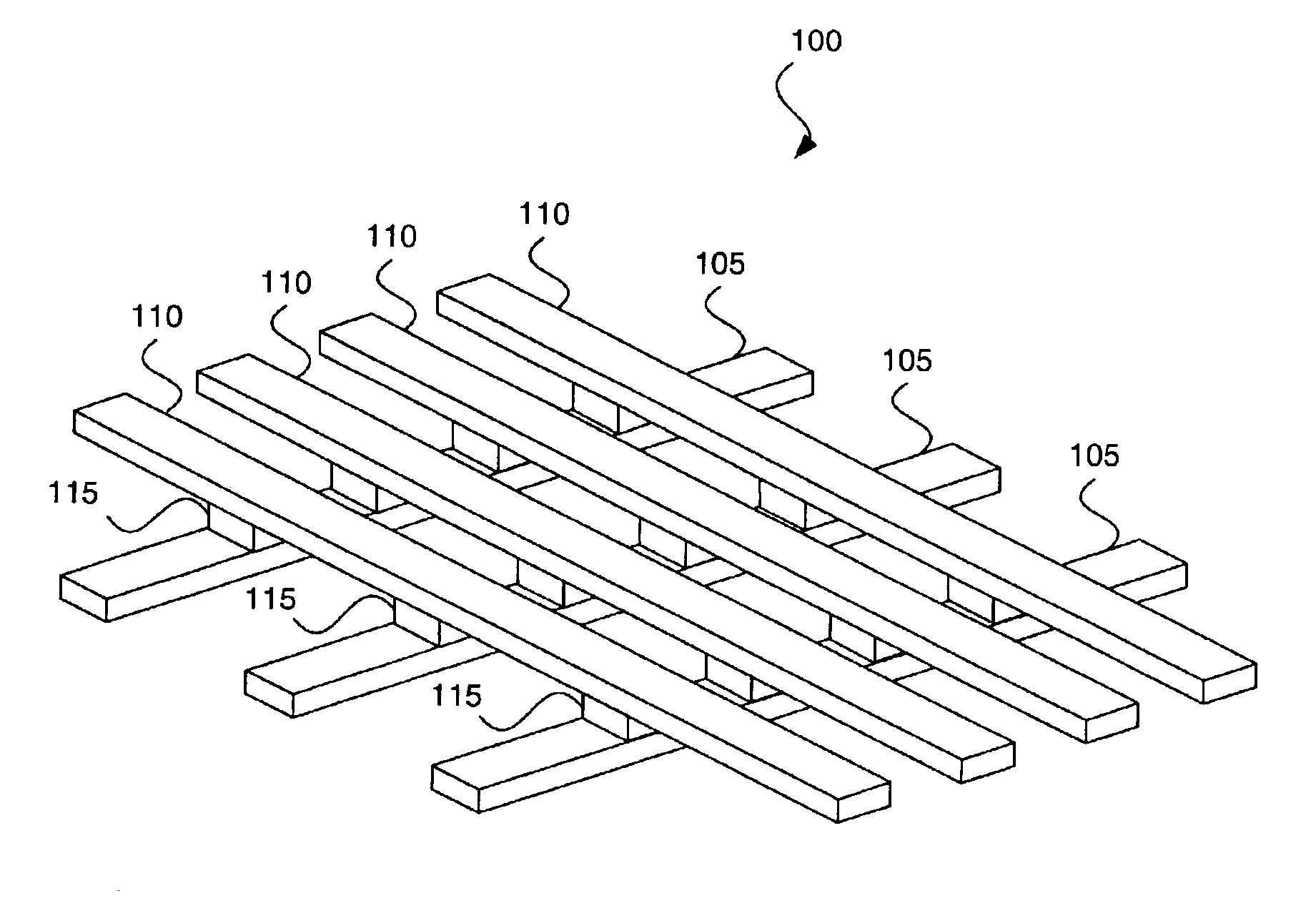
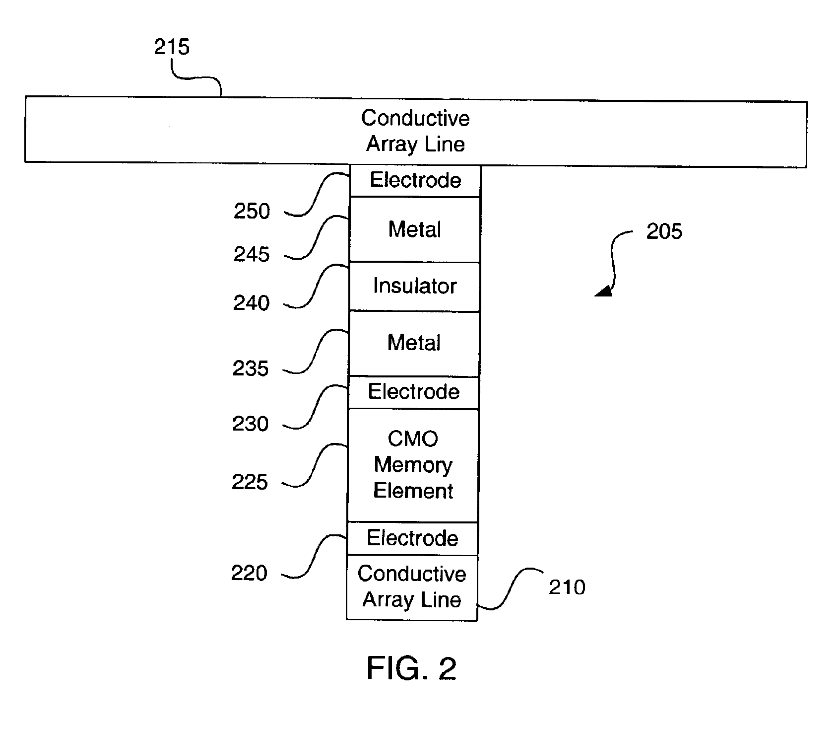
[0033]FIG. 1 depicts an exemplary cross point array 100. A bottom layer of x-direction conductive array lines 105 and a top layer of y-direction conductive array lines 110 sandwiches a plurality of memory plugs 115. The conductive array lines 105 and 110 are arranged in the cross point array 100 so that each individual memory plug is capable of being uniquely identified and, therefore, uniquely selected by a single x-direction conductive array line and a single y-direction conductive array line.

[0034]Conductive array lines 105 and 110 can be constructed of any conductive material, such as aluminum, copper, tungsten or certain ceramics. Ideally, the material will withstand a high-temperature fabrication process, have a low inherent resistance, and have a low cost. Often, however, compromises will have to be made.

[0035]For example, if the memory element is a CMO, very high temperatures might be required to form a polycrystalline or a single crystalline structure. Depending upon the fa...


PUM


Abstract

Providing a reference voltage to a cross point memory array. The invention is a cross point memory array and some peripheral circuitry that, when activated, provides a reference voltage to a cross point array in order to prevent unselected conductive array lines from floating to an undesired voltage. The peripheral circuitry can be activated before, after or during selection of a specific memory plug. If the peripheral circuitry is activated during selection, only the unselected conductive array lines should be brought to the reference voltage. Otherwise, all the conductive array lines can be brought to the reference voltage.

Description

CROSS-REFERENCE TO RELATED APPLICATIONS[0001]This application claims the benefit of U.S. Provisional Application No. 60 / 400,849, filed Aug. 02, 2002, the U.S. Provisional Application No. 60 / 422,922,filed Oct. 31, 2002, and the U.S. Provisional Application 60 / 424,083, filed Nov. 5, 2002, all of which are incorporated herein by reference in their entireties and for all purposes. This application is related to sister applications entitled “Cross Point Memory Array Using Multiple Thin Films,”U.S. Application No.: 10 / 330,512, filed Dec. 26, 2002, now Patent No. 6,753,561; “Cross Point Memory Array Using Multiple Modes of Operation,”U.S. Application No.: 10,330,153, filed Dec. 26, 2002, now Patent No. 6,834,008; “Cross Point Memory Array Using Distinct Voltages,” U.S. Application No. 10 / 330,964, filed Dec. 26, 2002, now Patent No. 6,831,854; “Cross Point Memory Array With Memory Plugs Exhibiting A Characteristic Hysteresis,”U.S. Application No.: 10,330,990, filed Dec. 26, 2002, now Pate...

Claims


Application Information

Patent Timeline
Patent Type & Authority Patents(United States)
IPC IPC(8): G11C13/00G11C16/02H01L27/24
CPCG11C5/147G11C11/15G11C13/0007G11C13/0004G11C2213/31
Inventor RINERSON, DARRELLCHEVALLIER, CHRISTOPHE J.LONGCOR, STEVEN W.WARD, EDMOND R.KINNEY, WAYNEHSIA, STEVE KUO-REN
Owner UNITY SEMICON
Why Eureka
Try Eureka