Methods and apparatus for packaging integrated circuit devices

a technology of integrated circuit devices and packaging dies, applied in electrical equipment, semiconductor devices, semiconductor/solid-state device details, etc., can solve the problems of poor bond formation of bonding and tabs, high temperature and mechanical pressure on dies, and problems such as the problem of wire bonding and tab technology

Inactive Publication Date: 2005-12-06
INVENSAS CORP +1
View PDF70 Cites 203 Cited by
  • Summary
  • Abstract
  • Description
  • Claims
  • Application Information

AI Technical Summary

Benefits of technology

[0021]In accordance with another preferred embodiment of the present invention the method also includes forming at least one gap in the plurality of dies and forming at least one chip scale packaging layer over the second generally planar surface, thereby sealing the gap.

Problems solved by technology

Both wire bonding and TAB bonding are prone to bad bond formation and subject the die to relatively high temperatures and mechanical pressures.
Both wire bond and TAB technologies are problematic from a package size viewpoint, producing integrated circuit devices having a die-to-package area ratio ranging from about 10% to 60%.
The flip-chip does not provide packaging but rather only interconnection.
The interconnection encounters problems of uniformity in the solder bumps as well as in thermal expansion mismatching, which limits available substrates to silicon or to materials which have thermal expansion characteristics similar to those of silicon.

Method used


Image

  • Methods and apparatus for packaging integrated circuit devices
  • Methods and apparatus for packaging integrated circuit devices
  • Methods and apparatus for packaging integrated circuit devices

Examples


Embodiment Construction

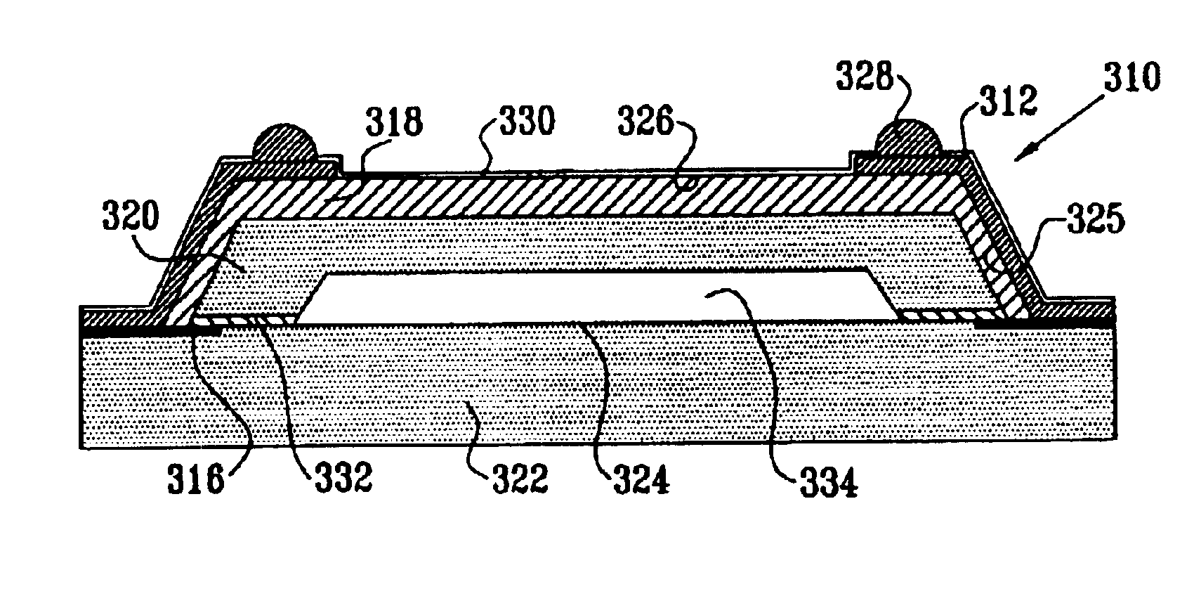
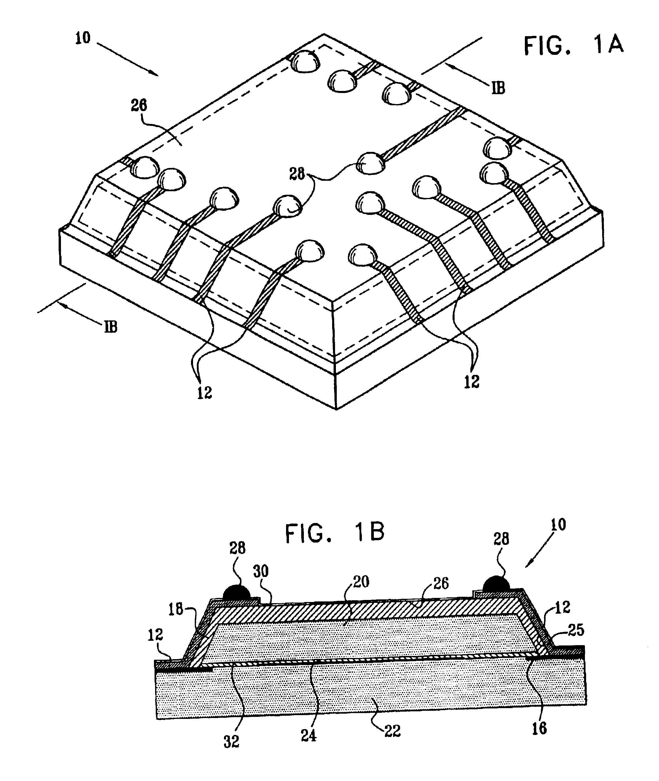
[0036]Reference is now made to FIGS. 1A-3J, which illustrate integrated circuit devices, and the production thereof, in accordance with a preferred embodiment of the present invention. As seen in FIGS. 1A and 1B, the integrated circuit device includes a relatively thin and compact, environmentally protected and mechanically strengthened, integrated circuit package 10, having a multiplicity of electrical conductors 12.

[0037]It is a particular feature of the present invention that conductors 12 are electrically connected to pads 16, and are preferably formed directly over an insulation layer 18 overlying at least one chip scale packaging layer 20 overlying an integrated circuit die 22 having an active surface 24. Alternatively insulation layer 18 may be partially or entirely obviated. Insulation layer 18 may be any suitable insulation layer, such as a dielectric layer or a passivation layer. Pads 16 are connected to circuitry on the active surface 24. Preferably the chip scale packagi...


PUM


Abstract

An integrally packaged integrated circuit device including an integrated circuit die including a crystalline substrate having first and second generally planar surfaces and edge surfaces and an active surface formed on the first generally planar surface, at least one chip scale packaging layer formed over the active surface and at least one electrical contact formed over the at least one chip scale packaging layer, the at least one electrical contact being connected to circuitry on the active surface by at least one pad formed on the first generally planar surface.

Description

FIELD OF THE INVENTION[0001]The present invention relates to methods and apparatus for producing integrated circuit devices and to integrated circuit devices produced thereby and more particularly to an integrally packaged die.BACKGROUND OF THE INVENTION[0002]An essential step in the manufacture of all integrated circuit devices is known as “packaging” and involves mechanical and environmental protection of a silicon chip which is at the heart of the integrated circuit as well as electrical interconnection between predetermined locations on the silicon chip and external electrical terminals.[0003]At present three principal technologies are employed for packaging semiconductors: wire bonding, tape automatic bonding (TAB) and flip chip.[0004]Wire bonding employs heat and ultrasonic energy to weld gold bonding wires between bond pads on the chip and contacts on the package.[0005]Tape automatic bonding (TAB) employs a copper foil tape instead of bonding wire. The copper foil tape is con...

Claims


Application Information

Patent Timeline
Patent Type & Authority Patents(United States)
IPC IPC(8): G01RH01L21/44H01L23/02H01L23/31H01L23/485H01L23/495
CPCH01L23/3114H01L24/94H01L24/13H01L24/11H01L2224/0401H01L24/12H01L2224/02321H01L2224/13099H01L2224/274H01L2924/01003H01L2924/01013H01L2924/01022H01L2924/01029H01L2924/01033H01L2924/01047H01L2924/01057H01L2924/01074H01L2924/01078H01L2924/01079H01L2924/01082H01L2924/01327H01L2924/14H01L2924/01005H01L2924/01006H01L2924/01024H01L2924/014H01L2224/02319H01L2224/024H01L2224/0236H01L2224/02335H01L2924/10253H01L2924/0001H01L2924/00H01L23/02
Inventor ZILBER, GILKATRARO, REUVENAKSENTON, JULIAOGANESIAN, VAGE
Owner INVENSAS CORP
Why Eureka
Try Eureka