Field emission array with carbon nanotubes and method for fabricating the field emission array

a carbon nanotube and field emission technology, applied in the manufacture of electrode systems, electric discharge tubes/lamps, tubes with screens, etc., can solve the problems of impurity gas, complicated fabrication process associated with thin film formation, etc., and achieve the effect of easy formation of thin films

Inactive Publication Date: 2005-12-20
SAMSUNG SDI CO LTD
View PDF22 Cites 50 Cited by
  • Summary
  • Abstract
  • Description
  • Claims
  • Application Information

AI Technical Summary

Benefits of technology

[0006]To solve the aforementioned problems, it is a feature of an embodiment of the present invention to provide a field emission array using carbon nanotubes as an electron emitter source, and a method for fabricating the field emission array, in which a nonconductive substrate with gates is built-in to a front substrate, and a rear substrate with cathodes and carbon nanotubes deposited on the cathodes, is combined with the front substrate assembly having the nonconductive substrate, so that the overall thin film formation becomes easy without causing generation of an impurity gas inside the field emission array during operation.

Problems solved by technology

For such triode-type electron emission devices with carbon nanotubes, the complicated fabrication process associated with thin film formation is considered a drawback.
Additionally, there is a problem of generating impurity gas inside a packaged device during operation.

Method used


Image

  • Field emission array with carbon nanotubes and method for fabricating the field emission array
  • Field emission array with carbon nanotubes and method for fabricating the field emission array
  • Field emission array with carbon nanotubes and method for fabricating the field emission array

Examples


first embodiment

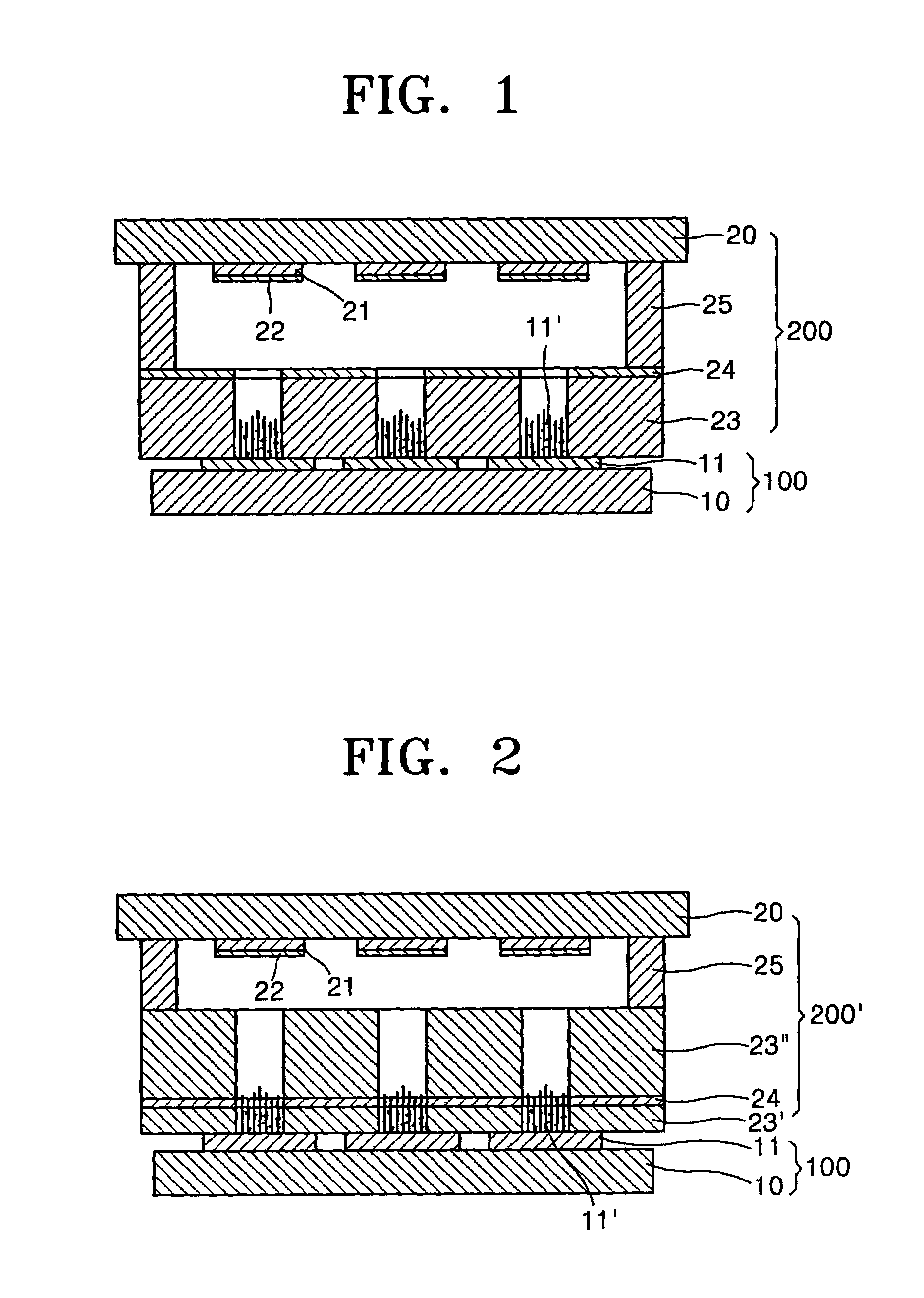
[0028]The field emission array fabrication according to the present invention has been described with reference to the configuration of the field emission array according to the present invention, illustrated in FIG. 1. Either the rear substrate assembly 100 or the front substrate assembly 200 can be manufactured first, i.e., prior to the manufacture of the other assembly.

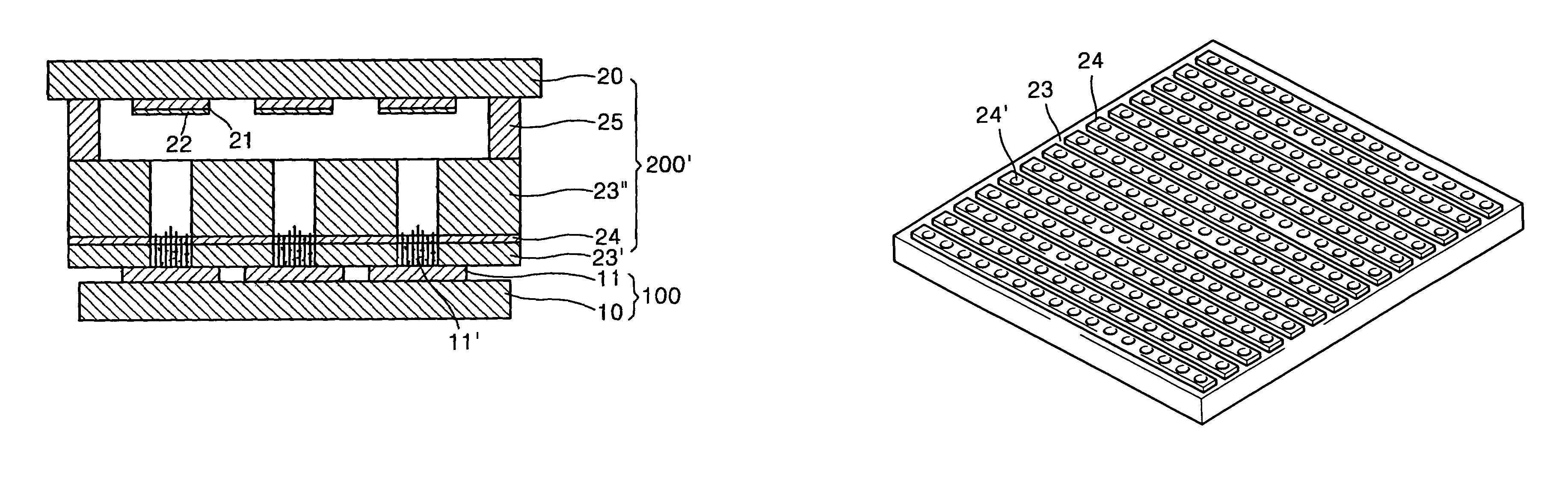
[0029]The fabrication of the field emission array according to the second embodiment, which is shown in FIG. 2, is the same as that of the first emission array shown in FIG. 1, except for the manufacture of the nonconductive plate 23. In particular, the gates 24 are formed as stripes over a first nonconductive plate 23′ relatively thinner than the nonconductive plate 23 for the first embodiment, and then a second nonconductive plate 23″ is mounted over the first nonconductive plate 23′ having gates 24.

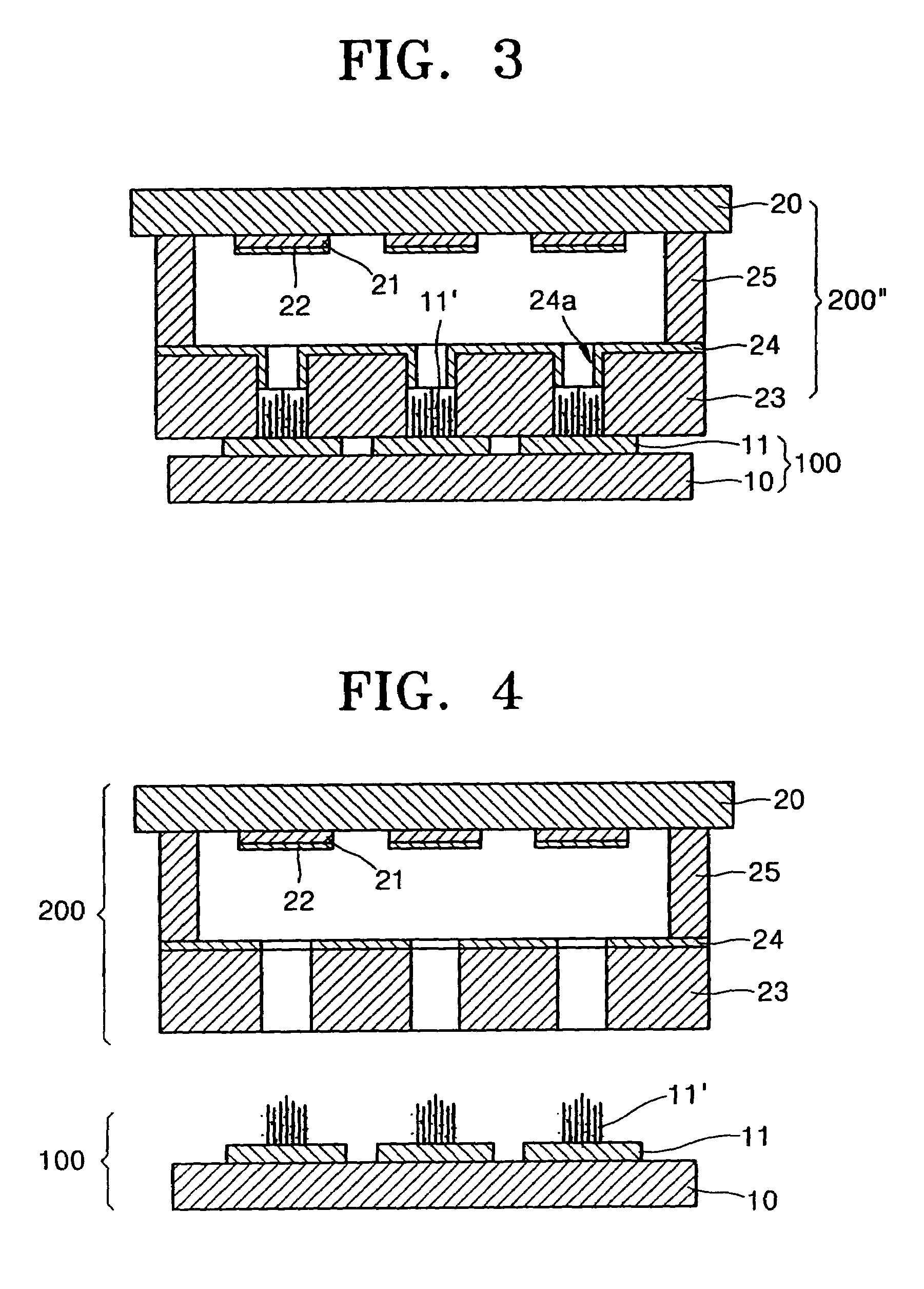
[0030]The fabrication of the field emission array according to the third embodiment of the present invention, which...

third embodiment

[0032]FIG. 10 is a graph illustrating the anode current flows at the field emission array according the present invention with respect to gate voltage variations at different anode voltage levels, the field emission array having gates formed by tilt deposition. As shown in FIG. 10, as the gate voltage level increases, anode current flow increases. The anode voltage level can be adjusted within the range of the gate voltage of 50–200 V.

[0033]As previously described, in the field emission array with carbon nanotubes as an electron emitter source, and the method for fabricating the field emission array according to the present invention, a rear substrate assembly is manufactured by forming cathodes as stripes on a rear substrate, and then by depositing carbon nanotubes on the cathodes. A front substrate assembly is manufactured by forming anodes as stripes on a front substrate and depositing a phosphor on the anodes; forming a plurality of openings in a nonconductive plate, and forming...


PUM

PropertyMeasurementUnit
anode voltageaaaaaaaaaa
brightnessaaaaaaaaaa

Abstract

A field emission array adopting carbon nanotubes as an electron emitter source, wherein the array includes a rear substrate assembly including cathodes formed as stripes over a rear substrate and carbon nanotubes; a front substrate assembly including anodes formed as stripes over a front substrate with phosphors being deposited on the anodes, a plurality of openings separated by a distance corresponding to the distance between the anodes in a nonconductive plate, and gates formed as stripes perpendicular to the stripes of anodes on the nonconductive plate with a plurality of emitter openings corresponding to the plurality of openings. The nonconductive plate is supported and separated from the front substrate using spacers. The rear substrate assembly is combined with the front substrate assembly such that the carbon nanotubes on the cathodes project through the emitter openings.

Description

CROSS REFERENCE TO RELATED APPLICATION(S)[0001]This is a divisional application based on application Ser. No. 09 / 837,225, filed Apr. 19, 2001 now U.S. Pat. No. 6,642,639, the entire contents of which is hereby incorporated by reference.BACKGROUND OF THE INVENTION[0002]1. Field of the Invention[0003]The present invention relates to a field emission array with carbon nanotubes as an electron emitter source, instead of conventional micro tips. The present invention further relates to a method for fabricating the field emission array of the present invention.[0004]2. Description of the Related Art[0005]In recent years, many attempts have been made to adopt carbon nanotubes as an electron emitter source in electron emission devices, instead of metallic micro tips, because the carbon nanotubes are superior in durability and thermal stability with a low work function. For such triode-type electron emission devices with carbon nanotubes, the complicated fabrication process associated with t...

Claims


Application Information

Patent Timeline
Patent Type & Authority Patents(United States)
IPC IPC(8): H01J9/24H01J1/304H01J3/02H01J5/03H01J9/02H01J29/04H01J29/87H01J31/12
CPCB82Y10/00H01J3/022H01J9/025H01J2201/30469H01J2329/00Y10S977/952C01B32/05H01J1/30B82Y40/00
Inventor CHOI, WON-BONGYUN, MIN-JAEJIN, YONG-WAN
Owner SAMSUNG SDI CO LTD
Why Eureka
Try Eureka