Data output control circuit

a control circuit and data output technology, applied in the field of semiconductor devices, can solve the problems of high increase, data output enable signal routen is not generated, time error between external clock signal and internal operating clock signal, etc., and achieve the effect of extended cas latency mode and operational speed drop

Active Publication Date: 2005-12-20
SK HYNIX INC
View PDF2 Cites 27 Cited by
  • Summary
  • Abstract
  • Description
  • Claims
  • Application Information

AI Technical Summary

Problems solved by technology

When the external clock signal is inputted to the synchronous semiconductor memory device in order to be used as the internal operating clock signal, there occurs a time error between the external clock signal and the internal operating clock signal.
Therefore, a rising time at the second node N′ is highly increased, and the rising data output enable signal routen is not generated at a proper timing.
In addition, an operational speed is slowed and a circuit of a semiconductor memory device is complicated.

Method used


Image

  • Data output control circuit
  • Data output control circuit
  • Data output control circuit

Examples


Embodiment Construction

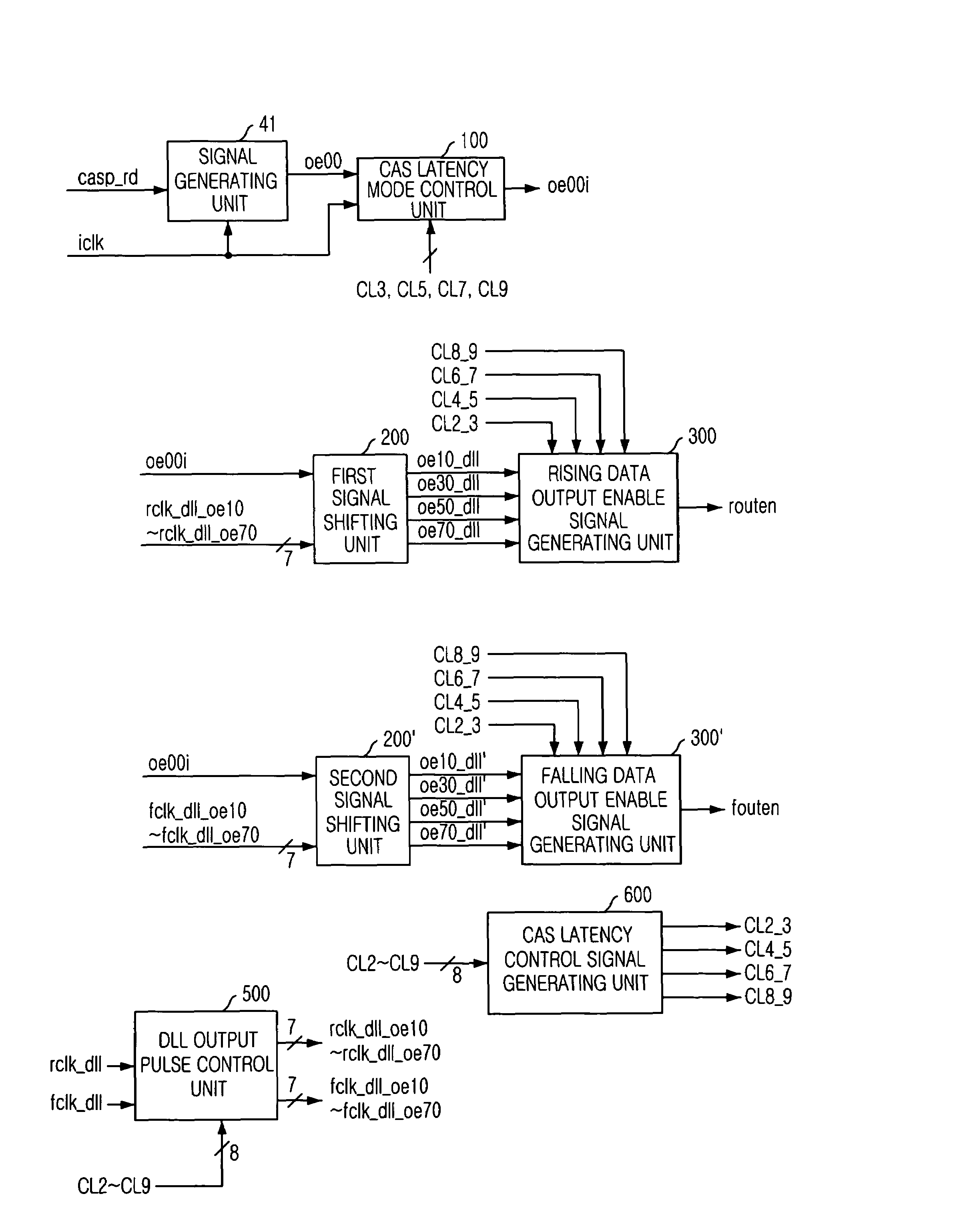
[0063]Hereinafter, a data output control circuit for use in a semiconductor memory device in accordance with the present invention will be described in detail referring to the accompanying drawings.

[0064]FIG. 5 is a block diagram showing a data output control circuit in accordance with a preferred embodiment of the present invention.

[0065]As shown, the data output control circuit includes a signal generating unit 41, a column address strobe (CAS) latency mode control unit 100, a first signal shifting unit 200, a rising data output enable signal generating unit 300, a second signal shifting unit 200′, a falling data output enable signal generating unit 300′, a CAS latency control signal generating unit 600 and a DLL output pulse control unit 500.

[0066]The signal generating unit 41 generates an internal signal oe00 in response to a read command performing signal casp—rd. The CAS latency mode control unit 100 receives the internal signal oe00 and outputs the received internal signal oe...


PUM


Abstract

A data output control circuit for use in a synchronous semiconductor memory device, which has a plurality of CAS latency modes, includes a signal generating unit for generating an internal signal corresponding to an input command; a CAS latency mode control unit for outputting the internal signal as a controlled internal signal; a signal shifting unit for generating a plurality of shifted signals by synchronizing the controlled internal signal with a DLL clock signal; and a data output enable signal generating unit for outputting one of the plurality of shifted signals as a data output enable signal depending on a plurality of control signals, wherein each of the plurality of control signals corresponds to two or more continuous CAS latency modes.

Description

FIELD OF THE INVENTION[0001]The present invention relates to a semiconductor device; and, more particularly, to a data output control circuit for generating a data output enable signal.DESCRIPTION OF THE PRIOR ART[0002]A semiconductor memory device has been continuously improved to increase its operational speed. One of methods to improve an operational speed of a semiconductor memory device is to make the semiconductor memory device operate in synchronization with an external clock signal. Therefore, a semiconductor memory device which operates in synchronization with the external clock signal, namely a synchronous semiconductor memory device, has been developed.[0003]The synchronous semiconductor memory device performs a data access operation at a rising edge of the external clock signal. That is, the synchronous semiconductor memory device can perform the data access operation once within one cycle of the external clock signal.[0004]Such a synchronous semiconductor memory device ...

Claims


Application Information

Patent Timeline
Patent Type & Authority Patents(United States)
IPC IPC(8): G11C11/40G11C7/00G11C7/10G11C8/00G11C11/34
CPCG11C7/103G11C7/1051G11C7/106G11C7/1066G11C11/40
Inventor CHOI, YOUNG-BAE
Owner SK HYNIX INC
Why Eureka
Try Eureka